Tunnel effect transistors based on silicon nanowires

a technology of tunnel field effect transistor and silicon nanowire, which is applied in the direction of nanotechnology, electrical equipment, nanotechnology, etc., can solve the problems of low on-current tfet, difficulty in reducing supply voltage, and increasing power consumption, so as to improve the architecture and low power consumption

Inactive Publication Date: 2008-03-20
KATHOLIEKE UNIV LEUVEN
View PDF10 Cites 122 Cited by
  • Summary
  • Abstract
  • Description
  • Claims
  • Application Information

AI Technical Summary

Benefits of technology

[0009]It is an object of the present invention to provide semiconductor device structures with an improved architecture and having lo...

Problems solved by technology

One of the problems due to the scaling down of CMOS transistors is that the power consumption keeps increasing.
This is partly because leakage currents are increasing (e.g. due to short channel effects) and because it becomes difficult to decrease the supply voltage.
However, TFETs typically suffer from lo...

Method used


Image

  • Tunnel effect transistors based on silicon nanowires
  • Tunnel effect transistors based on silicon nanowires
  • Tunnel effect transistors based on silicon nanowires

Examples


example 1

Simulations with Device Simulator MEDICI to Determine the Characteristics of a (Silicon) NW-TFET with a Highly-Doped Ge Section at the Tunnel Barrier

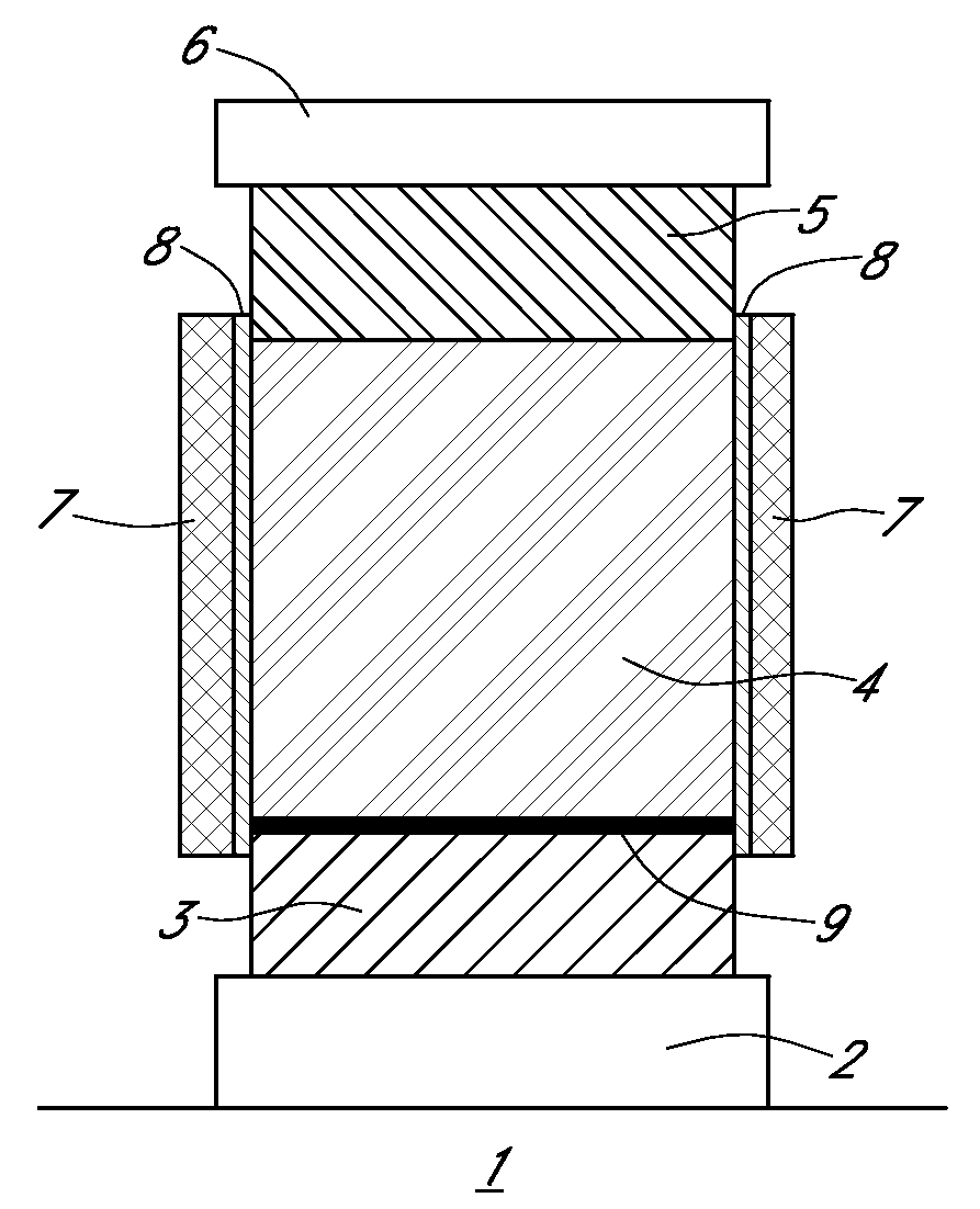
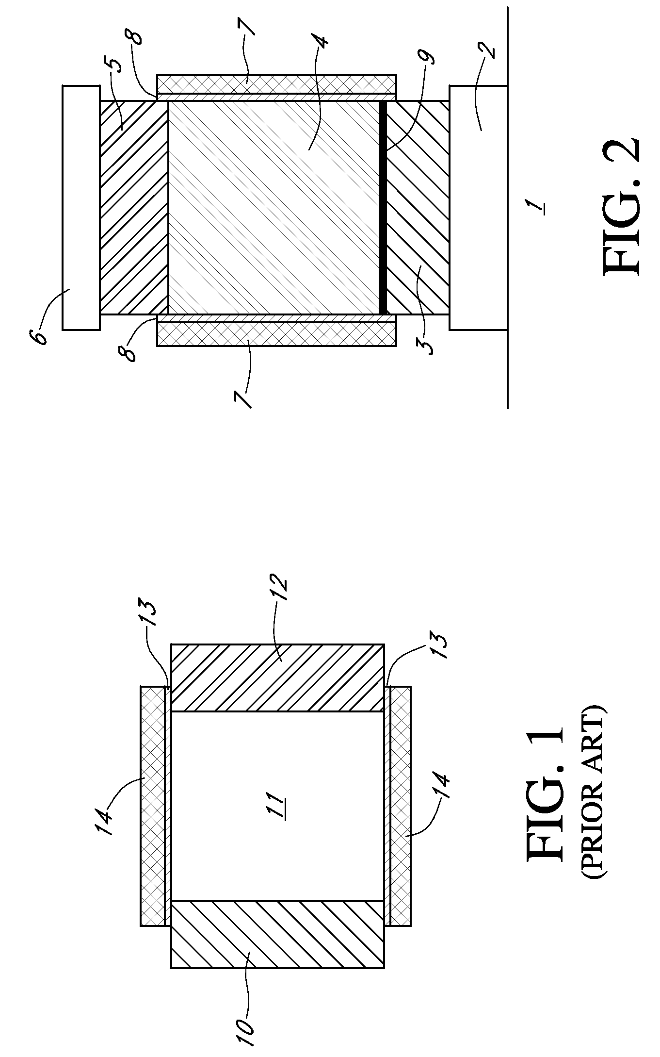
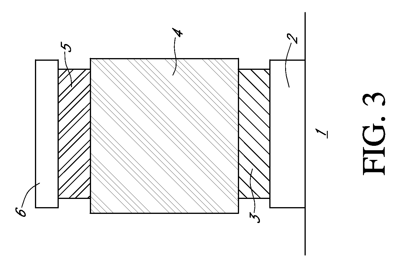
[0108]TFETs typically suffer from low on-currents, a drawback related to the large resistance of the tunnel barrier. This simulation illustrated below demonstrates that high on-currents can be achieved for a TFET with a germanium (Ge) tunnel barrier in an otherwise silicon (Si) channel. Such a configuration is only possible when nanowires are used, such that the lattice mismatch between silicon and germanium does not result in a highly defective interface. The simulations predict a dynamic power reduction of up to a factor of at least 5, as well as a static power reduction of at least a factor of 2 compared to conventional MOSFET configurations. Multiple layers of logic can therefore be envisioned with these nanowire Si / Ge TFETs resulting in ultra-high on-chip transistor densities.

[0109]The simulations are performed with device simulato...


PUM


Abstract

Tunnel field-effect transistors (TFETs) are regarded as successors of metal-oxide semiconductor field-effect transistors (MOSFETs), but silicon-based TFETs typically suffer from low on-currents, a drawback related to the large resistance of the tunnel barrier. To achieve higher on-currents a nanowire-based TFET with a germanium (Ge) tunnel barrier in an otherwise silicon (Si) channel is used. A nanowire is introduced such that the lattice mismatch between silicon and germanium does not result in a highly defective interface. A dynamic power reduction as well as a static power reduction can result, compared to conventional MOSFET configurations. Multiple layers of logic can therefore be envisioned with these nanowire Si/Ge TFETs resulting in ultra-high on-chip transistor densities.

Description

CROSS-REFERENCE TO RELATED APPLICATIONS[0001]This application claims the benefit under 35 U.S.C. § 119(e) of U.S. provisional application Ser. No. 60 / 845,006, filed Sep. 15, 2006, and claims the benefit under 35 U.S.C. § 119(a)-(d) of European application No. EP 06024507.3, filed Nov. 27, 2006, the disclosures of which are hereby expressly incorporated by reference in their entireties and are hereby expressly made a portion of this application.FIELD OF THE INVENTION[0002]The present invention is related to the field of semiconductor devices and nanotechnology. More specifically, the invention is related to a nanostructure semiconductor device, more specifically to a tunnel field effect transistor having a heterostructure nanowire, and a method for manufacturing such tunnel field effect transistor devices with integrated nanowires.BACKGROUND OF THE INVENTION[0003]Microelectronic devices are generally fabricated on semiconductor substrates as integrated circuits. A complementary metal...

Claims


Application Information

Patent Timeline
IPC IPC(8): H01L29/775H01L21/336
CPCB82Y10/00H01L29/0665H01L29/0673H01L29/7391H01L29/068H01L29/165H01L29/66977H01L29/0676Y10S977/762Y10S977/70
Inventor VERHULST, ANNE S.
Owner KATHOLIEKE UNIV LEUVEN
Why Eureka
Try Eureka