Tunnel effect transistors based on elongate monocrystalline nanostructures having a heterostructure

a monocrystalline nanostructure and tunnel effect technology, applied in the field of tunnel field effect transistors, can solve the problems of difficult to reduce the supply voltage, low on-current of tfets, and increase power consumption, and achieve the effect of low power consumption

Active Publication Date: 2011-12-06
KATHOLIEKE UNIV LEUVEN +1
View PDF22 Cites 15 Cited by
  • Summary
  • Abstract
  • Description
  • Claims
  • Application Information

AI Technical Summary

Benefits of technology

[0009]Semiconductor device structures are provided with an improved architecture and having low power consumption using elongate monocrystalline nanostructures such as nanowires. A method for the manufacturing of such semiconductor device structures is also provided.
[0011]It is further an advantage of the NW-TFET of the preferred embodiments that Si based materials and process knowledge can be used to create the NW-TFET such that the NW-TFET can be easily processed and incorporated in current Si-based technology devices.
[0012]Preferred embodiments relate to micro and nanoelectronics and may be used for developing low power semiconductor device structures. Using the tunnel field effect transistor of the preferred embodiments it is possible to increase the number of transistors on a chip further. The elongate monocrystalline nanostructure tunnel field effect transistor, e.g. nanowire tunnel field effect transistor of some embodiments of the preferred embodiments can be based on current Si based technology and can therefore be easily incorporated in current devices using current state of the art technologies. The elongate monocrystalline nanostructure tunnel field effect transistor, e.g., nanowire tunnel field effect transistor, of some of the embodiments is distinguished from all analogous TFETs known in prior art by the integration of an appropriate heterosection. A heterosection is a section along the longitudinal axis of an elongate monocrystalline nanostructure, e.g. nanowire, which is made of a material which is different from the material of the main part of the elongate monocrystalline nanostructure. The heterosection can help enable an improved performance in terms of any or all of: high ON currents (the resistance associated with the tunnel barrier can be decreased by using a material with a very small bandgap for the heterosection and / or a material with a different electron affinity for the heterosection than the electron affinity of the material of the main part of the elongate monocrystalline nanostructure), low OFF currents (the off-current is determined by the material of the main part of the elongate monocrystalline nanostructure, and can be chosen independently of the material of the heterosection) and fast OFF-to-ON transition (as simulations have indicated, in the presence of a heterosection, whereby the heterosection material has a smaller bandgap than the material of the main part of the elongate monocrystalline nanostructure, or whereby the heterosection material has a different electron affinity from the electron affinity of the material of the main part of the elongate monocrystalline nanostructure, the OFF-to-ON transition becomes faster). The interface between the material of the main part of the elongate monocrystalline nanostructure and the heterosection can be substantially defect-free, i.e. it does not result in a highly defective interface, because this is an elongate monocrystalline nanostructure and the very small cross section allows for efficient lateral stress relaxation. An example is a silicon nanowire with a germanium heterosection, where the lattice mismatch between silicon and germanium does not result in a highly defective interface.
[0013]In a preferred embodiment, a Tunnel Field Effect Transistor (TFET) semiconductor device is provided. Said TFET comprises at least one elongate monocrystalline nanostructure, e.g. nanowire (to form a NW-TFET) or a semiconducting carbon nanotube, said elongate monocrystalline nanostructure further comprising at least one drain (alternatively source) region made of a first semiconductor material which is highly doped according to a first conductivity type, e.g. p doped (or n doped), at least one heterosection acting as source (alternatively drain) region made of a second semiconductor material which is highly doped according to a second conductivity type, e.g. n doped (or p doped) and at least one channel region made of a first semiconductor material which is lowly doped according to the first conductivity type or the second conductivity type, e.g. n doped or p doped, and which is situated in between the source and drain region. The latter embodiment is possible because an elongate monocrystalline nanostructure, e.g. nanowire, can have sufficiently defect-free heterosections of arbitrary length. The latter embodiment has the advantage that it requires one less processing step in the fabrication of the Tunnel Field Effect Transistor (NW-TFET), as the source region (or drain region) is made of only one material.

Problems solved by technology

One of the problems due to the scaling down of CMOS transistors is that the power consumption keeps increasing.
This is partly because leakage currents are increasing (e.g. due to short channel effects) and because it becomes difficult to decrease the supply voltage.
However, TFETs typically suffer from low on-currents, a drawback related to the large resistance of the tunnel barrier.
The proposed structure still has the disadvantage of introducing new materials (carbon nanotubes).
However, these structures with the Si1-xGex section can still not compete with conventional MOSFETs because of their low on-currents.

Method used


Image

  • Tunnel effect transistors based on elongate monocrystalline nanostructures having a heterostructure
  • Tunnel effect transistors based on elongate monocrystalline nanostructures having a heterostructure
  • Tunnel effect transistors based on elongate monocrystalline nanostructures having a heterostructure

Examples


example 1

Simulations with Device Simulator MEDICI to Illustrate the Effect of Electron Affinity on a (Silicon) N-type NW-TFET with a Highly P-doped Ge Heterosection.

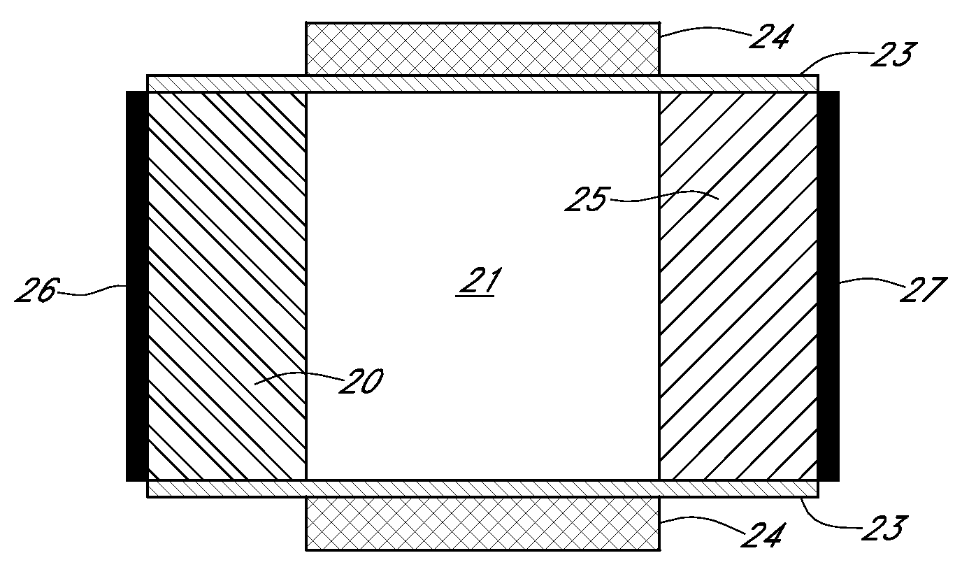
[0109]The simulations are performed with device simulator “MEDICI” to illustrate the effect of electron affinity on a (silicon) n-type NW-TFET with a highly p-doped Ge heterosection. The NW-TFET used for the simulation is shown in FIG. 6A. The NW-TFET structure is 2-dimensional and has a double-gate 24. The height of the central part (between the oxides) is 100 nm, and the height of the hafnium oxide 23 is 4 nm. The width of the highly p-doped heterosection 25 which forms the source region is 30 nm, the width of the channel region 21 is 60 nm, and the width of the highly n-doped drain 22 section is 30 nm. The heterosection 25 is made of either Si0Ge1 or Ge. The definition of Si0Ge1 in MEDICI is: an artificial material with the bandgap of Ge but with the electron affinity of Si. The doping concentrations and dopant type in the NW-...

example 2

Simulations with Device Simulator MEDICI to Illustrate the Effect of Electron Affinity on a (Silicon) P-type NW-TFET with a Highly N-doped Heterosection.

[0112]The simulations are performed with device simulator “MEDICI” to illustrate the effect of electron affinity on a (silicon) p-type NW-TFET with a highly n-doped heterosection. The NW-TFET used for the simulation is shown in FIG. 7A. The NW-TFET structure is 2-dimensional and has a double-gate 24. The height of the central part (between the oxides) is 100 nm, and the height of the hafnium gate 23 oxide is 4 nm. The width of the highly p-doped source region 20 is 30 nm, the width of the channel region 21 is 100 nm, and the width of the highly n-doped heterosection 25 which forms the drain region is 30 nm. The heterosection 25 is made of either Si or of an artificial material X which has all properties of Si except for a larger electron affinity (Eaff,X=4.69 eV, instead of the correct value of Eaff,Si=4.17 eV). The doping concentra...


PUM


Abstract

Tunnel field-effect transistors (TFETs) are regarded as successors of metal-oxide semiconductor field-effect transistors (MOSFETs), but silicon-based TFETs typically suffer from low on-currents, a drawback related to the large resistance of the tunnel barrier. To achieve higher on-currents an elongate monocrystalline nanostructure-based TFET with a heterostructure made of a different semiconducting material (e.g. germanium (Ge)) is used. An elongate monocrystalline nanostructure made of a different semiconducting material is introduced which acts as source (or alternatively drain) region of the TFET. The introduction of the heterosection is such that the lattice mismatch between silicon and germanium does not result in a highly defective interface. A dynamic power reduction as well as a static power reduction can result, compared to conventional MOSFET configurations. Multiple layers of logic can therefore be envisioned with these elongate monocrystalline nanostructure Si / Ge TFETs resulting in ultra-high on-chip transistor densities.

Description

CROSS-REFERENCE TO RELATED APPLICATIONS[0001]This application claims the benefit under 35 U.S.C. §119(e) of U.S. provisional application Ser. No. 60 / 845,006 filed Sep. 15, 2006, the disclosure of which is hereby expressly incorporated by reference in its entirety and is hereby expressly made a portion of this application.FIELD OF THE INVENTION[0002]The present invention is related to the field of semiconductor devices and nanotechnology. More specifically, the invention is related to a nanostructure semiconductor device, more specifically to a tunnel field effect transistor having an elongate monocrystalline heterostructure nanostructure, e.g. nanowire, and a method for manufacturing such tunnel field effect transistor devices with integrated elongate monocrystalline nanostructures.BACKGROUND OF THE INVENTION[0003]Microelectronic devices are generally fabricated on semiconductor substrates as integrated circuits. A complementary metal-oxide-semiconductor (CMOS) field effect transist...

Claims


Application Information

Patent Timeline
Patent Type & Authority Patents(United States)
IPC IPC(8): H01L29/94H01L21/8238
CPCB82Y10/00H01L29/0665H01L29/7391H01L29/0676H01L29/068H01L29/0673
Inventor VERHULST, ANNE S.VANDENBERGHE, WILLIAM G.
Owner KATHOLIEKE UNIV LEUVEN
Why Eureka
Try Eureka