Semiconductor device

a technology of semiconductor devices and semiconductors, applied in semiconductor devices, instruments, electrical devices, etc., can solve the problems of difficulty in writing and erasing, and the time required for writing and erasing exceeds the range acceptable for practical us

Active Publication Date: 2008-03-27
RENESAS ELECTRONICS CORP
View PDF15 Cites 16 Cited by
  • Summary
  • Abstract
  • Description
  • Claims
  • Application Information

AI Technical Summary

Benefits of technology

[0007]For its prevention, a method in which charges of different polarity are injected using hot carriers instead of emitting the charges, thereby rewriting the stored data has been proposed. In this method, since the hot carrier injection is used, the charge injection can be efficiently performed even when a thick insulator is formed.
[0029]Therefore, an object of the present invention is to provide a technology capable of improving the electric characteristics of a semiconductor device having a non-volatile memory structure.
[0036]That is, an insulator gate field effect transistor structure in which a field effect is applied to a substrate surface by a gate electrode formed on the substrate via a gate dielectric comprises a non-volatile memory element using the gate dielectric as a charge-trapping layer, in which the gate dielectric has a structure in which a first insulator, a second insulator, a third insulator, and a fourth insulator are laminated in this order from the substrate side, and the third insulator has a bandgap larger than a bandgap of the second insulator and has an energy barrier to the charges. Accordingly, it is possible to improve the electric characteristics of a semiconductor device having the non-volatile memory structure.

Problems solved by technology

However, the pursuit of the sufficient charge-trapping characteristics while performing the charge injection and emission basically causes some problems.
For example, in an actual use, when the thickness of the laminated film is increased in order to have sufficient charge-trapping characteristics, the writing and erasing become difficult, and the time required for the writing and erasing exceeds the range acceptable for the practical use.

Method used


Image

  • Semiconductor device
  • Semiconductor device
  • Semiconductor device

Examples


first embodiment

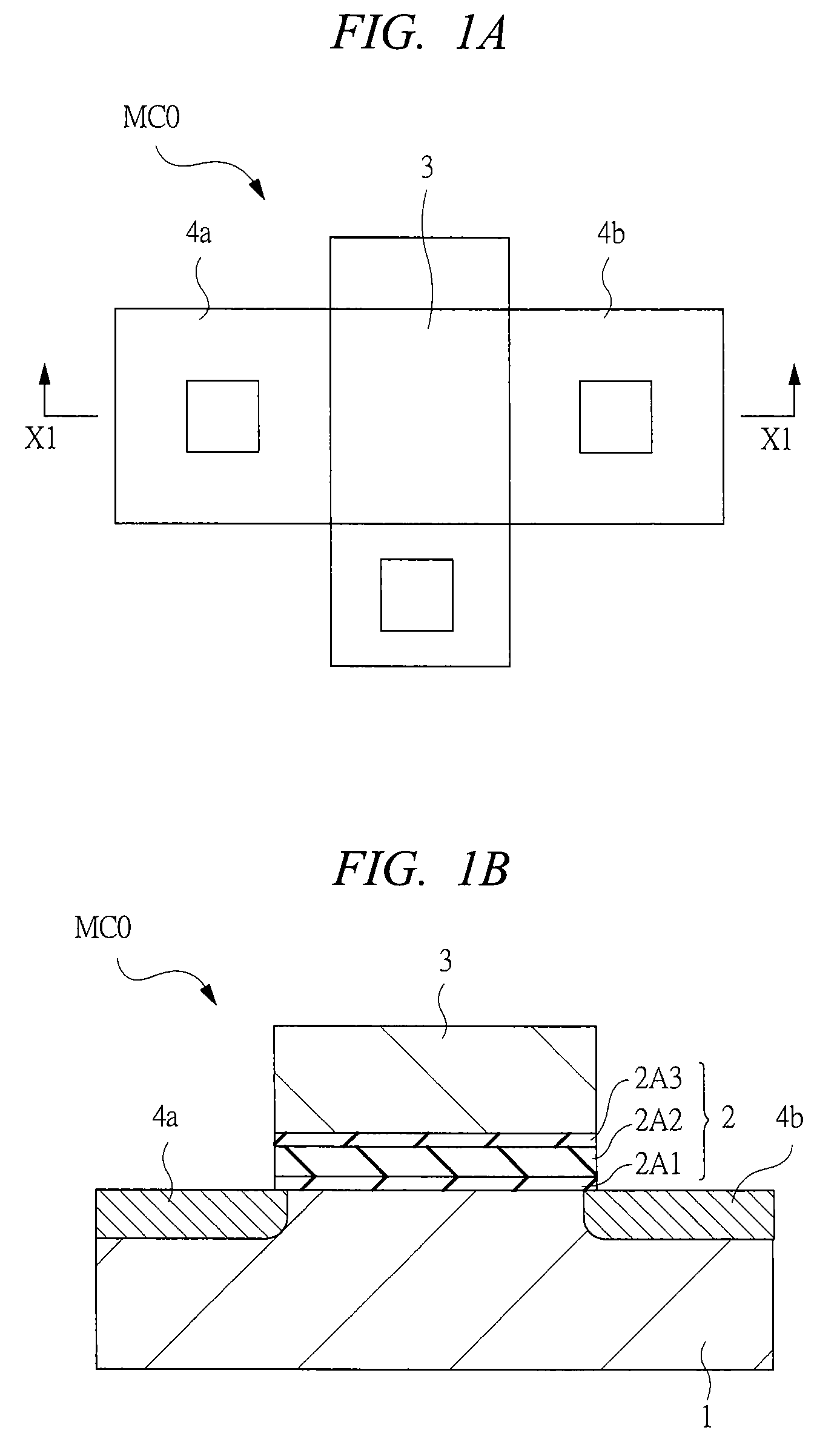
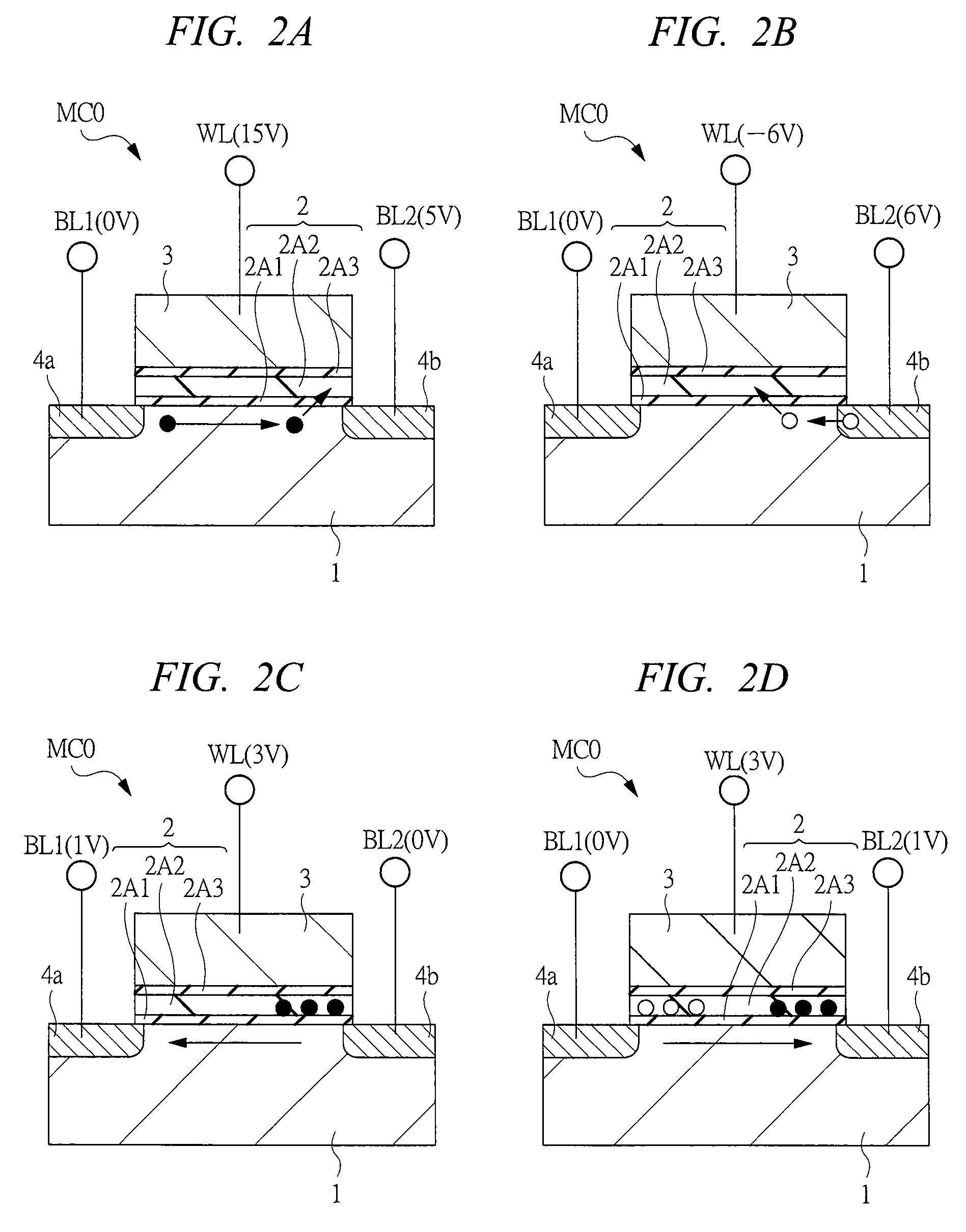
[0081]The hole injection from the gate electrode side which is the feature of the first embodiment can be understood by the one-dimensional band structure in a direction vertical to the substrate. Therefore, in the first embodiment, the case of using a non-volatile memory cell (hereinafter, simply referred to as memory cell in the embodiments below) having the same device structure as a normal MOSFET (Metal Oxide Field Effect Transistor) whose structure is characteristic will be described as a typical cell structure. Thereafter, the electron injection method will be examined, and the case where it is used for the cell structure suitable for high-speed operation will be described. In these cases, optimal structure can be selected and used in accordance with the use of the memory cell.

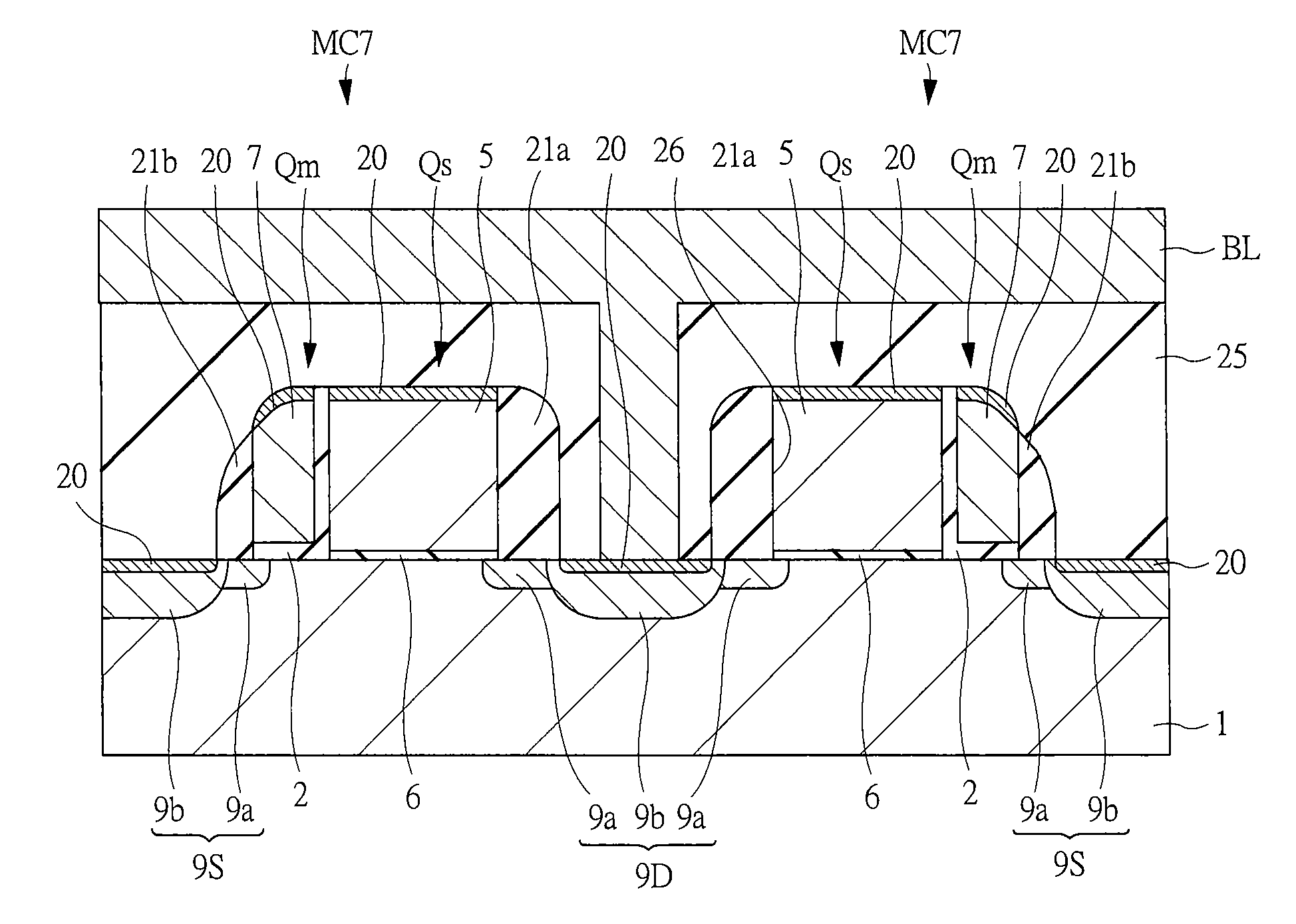
[0082]The manufacturing process of a semiconductor device having a non-volatile memory according to the first embodiment will be described below with reference to FIG. 7 to FIG. 10. By this means, the st...

second embodiment

[0105]As is apparent from the first embodiment, it is necessary to suppress the discharge by using an insulator having an energy barrier for the charge-trapping layer (insulator 2B2) in order to maintain the charge-trapping characteristics.

[0106]According to the first embodiment, the insulator 2B1 formed of a silicon oxide film is used for a lower side (substrate side) where the hot-carrier injection of electrons can be achieved. Therefore, good barrier characteristics can be obtained. Accordingly, in the second embodiment, a film structure capable of achieving both the charge-trapping characteristics and hole injection will be considered for an upper side (gate electrode side).

[0107]More specifically, by using a film having a large bandgap for a charge-trapping layer, a large band offset can be obtained. On the other hand, when considering the hole injection, it is required that the energy barrier from the gate electrode is lower than that of a silicon substrate and a silicon oxide...

third embodiment

[0111]The first embodiment has described that the energy barrier can be provided to the charge-trapping layer (insulator 2B2) by forming a silicon nitride film containing oxygen.

[0112]In the third embodiment, the case where a charge-trapping layer of a memory cell is formed of a silicon nitride film having large silicon composition will be described. The silicon nitride film having large silicon composition has a bandgap smaller than that of a (normal) silicon nitride film of stoichiometric composition. The band structure of the gate dielectric 2 in this case is shown in FIG. 15. Also, FIG. 15 shows the flat-band state (state where no bias is applied to the gate dielectric 2 between the gate electrode 3 and the substrate 1, that is, state where electric field of the gate dielectric 2 having no charge is zero or electric field of the channel surface is zero).

[0113]In the memory cell MC4 according to the third embodiment, the insulator 2B5 functioning as a charge-trapping layer is for...


PUM


Abstract

A gate dielectric functioning as a charge-trapping layer of a non-volatile memory cell with a structure of an insulator gate field effect transistor is formed by laminating a first insulator formed of a silicon oxide film, a second insulator formed of a silicon nitride film, a third insulator formed of a silicon nitride film containing oxygen, and a fourth insulator formed of a silicon oxide film in this order on a main surface of a semiconductor substrate. Holes are injected into the charge-trapping layer from a gate electrode side. Accordingly, since the operations can be achieved without the penetration of the holes through the interface in contact to the channel and the first insulator, the deterioration in rewriting endurance and the charge-trapping characteristics due to the deterioration of the first insulator does not occur, and highly efficient rewriting (writing and erasing) characteristics and stable charge-trapping characteristics can be achieved.

Description

CROSS-REFERENCE TO RELATED APPLICATION[0001]The present application claims priority from Japanese Patent Application No. JP 2006-255884 filed on Sep. 21, 2006, the content of which is hereby incorporated by reference into this application.TECHNICAL FIELD OF THE INVENTION[0002]The present invention relates to a technology for a semiconductor device. More particularly, it relates to a method for effectively operating a device having a non-volatile memory structure.BACKGROUND OF THE INVENTION[0003]At present, an LSI (Large Scale Integration) in which semiconductor elements are integrated has been used for various system controls and has become a basic infrastructure for society. Since the recent LSI is operated on the basis of the arithmetic processing in accordance with programs, the condition that program can be stored is indispensable in many cases, and a non-volatile memory which is one type of integrated semiconductor memories incorporated in an LSI has become extremely important ...

Claims


Application Information

Patent Timeline
Patent Type & Authority Applications(United States)
IPC IPC(8): H01L29/792
CPCG11C16/0425G11C16/10H01L29/792H01L27/11568H01L29/66833H01L27/115H10B43/30H10B69/00
Inventor HISAMOTO, DIGHYANAGI, ITARUSHIMAMOTO, YASUHIROMINE, TOSHIYUKIOKUYAMA, YUTAKA
Owner RENESAS ELECTRONICS CORP
Why Eureka
Try Eureka