Semiconductor device

a semiconductor device and semiconductor technology, applied in the direction of semiconductor devices, basic electric elements, electrical equipment, etc., can solve the problems of variable problems, achieve the effect of reducing the thickness of the silicon substrate, reducing the withstand voltage decline of the semiconductor device, and controlling the concentration of the electric field

Inactive Publication Date: 2008-03-27
LAPIS SEMICON CO LTD
View PDF6 Cites 14 Cited by
  • Summary
  • Abstract
  • Description
  • Claims
  • Application Information

AI Technical Summary

Benefits of technology

[0009]Further, another object of the present invention is to provide a method of manufacturing a semiconductor device which is able to control the concentration of the electric field in the insulation film under the field plate electrode.
[0011]According to the present invention, the end shape of the insulation film under the field plate electrode is moderately inclined. Here, the field plate structure is a structure where a field plate electrode of the same electric potential as that of the gate electrode is formed on the protective film between the gate electrode and the drain electrode of a transistor, and thereby reducing the concentration of the electric field in the gate electrode end during the operation and obtaining high withstand voltage, and high output.
[0018]According to the present invention, it is possible to form the end shape of the insulation film under the field plate electrode moderately inclined, and control the concentration of the electric field generated at the end of the insulation film under the field plate electrode effectively. As a result, it is possible to restrain the withstand voltage decline of a semiconductor device.
[0019]The protective insulation film under the gate field plate is not formed inside the silicon substrate, and accordingly the flatness of the silicon substrate surface is maintained. Further, the protective insulation film has a moderate inclination at the end thereof, and the protective film thickness under the gate electrode does not change sharply. Furthermore, it is possible to determine the film thickness of the protective insulation film independently from the field oxide film thickness for isolation, and distribute the electric field under the best conditions. As a result, it becomes possible to prevent such a withstand voltage decline by the concentration of the electric field in the oxide film end as seen in the conventional art.
[0020]When the isotropic wet etching method is employed for forming the protective insulation film on the semiconductor substrate, there is no necessity of using the silicone epitaxial growth method and the high-density plasma CVD method, and accordingly it is possible to form the protective insulation film at low cost.
[0021]On the other hand, according to the second and the fifth aspects of the present invention mentioned above, the protective insulation film is formed by the LOCOS method in the same manner as the isolation region, and the protective insulation film is thinner in thickness, and the shape of bird's beak becomes moderate. Therefore, the flatness of the semiconductor substrate surface is maintained more than in the conventional art, and it becomes possible to prevent the withstand voltage decline by the concentration of the electric field at the end of the protective insulation film. Moreover, it becomes possible to form field oxide films which have different film thickness values by one photolithography process, and restrain the increase of manufacturing cost.

Problems solved by technology

However, in the semiconductor device of the configuration shown above, since the field oxide film on which the gate electrode lies is formed simultaneously with other field oxide films used for isolation, various problems have occurred.

Method used


Image

  • Semiconductor device
  • Semiconductor device
  • Semiconductor device

Examples


first embodiment

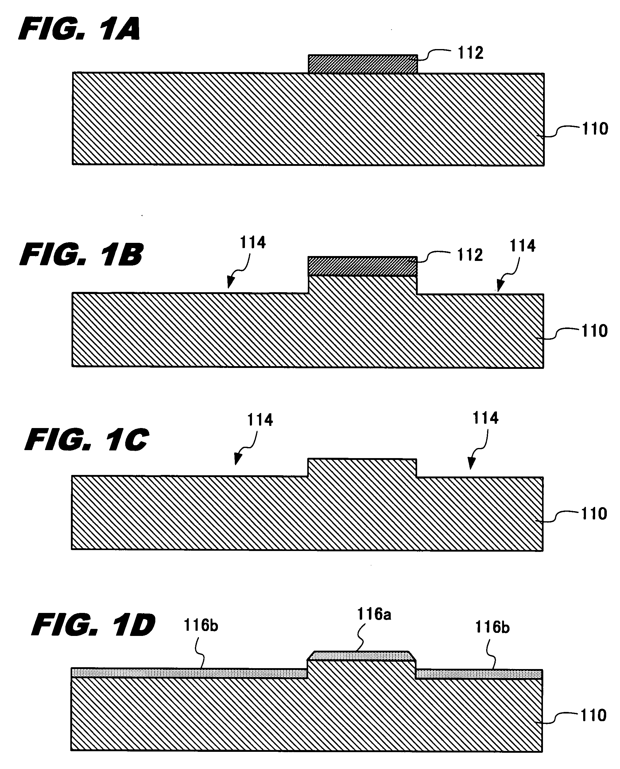
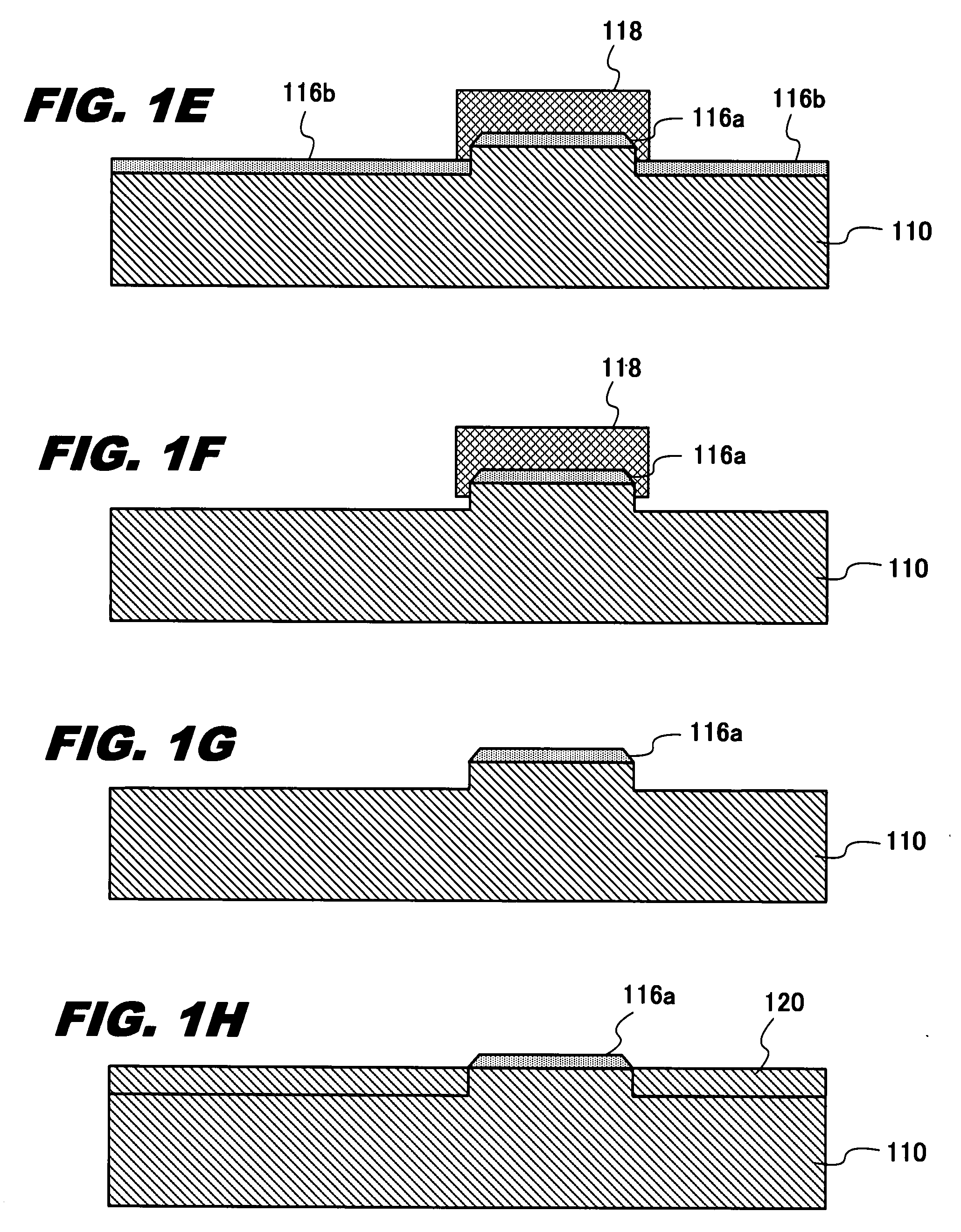
[0039]A semiconductor device according to a first embodiment of the present invention has a gate field plate structure. As explained later herein, a silicone oxide film (protective insulation) on which a part of a gate electrode lies is formed by other method than the LOCOS oxidizing method, and the flatness of a silicon substrate surface is maintained. Furthermore, it is characterized by that the inclination of the end of the silicone oxide film (protective insulation film) is moderate, and the oxide film thickness under the gate electrode does not change sharply.

[0040]FIGS. 1A-1N are cross sectional views each showing a method of manufacturing a LDMOS (lateral diffused MOS) to become a semiconductor device according to the first embodiment of the present invention.

[0041]First, as shown in FIG. 1A, a photo resist 112 is patterned on an N type silicon substrate 10 by photolithography techniques.

[0042]Next, as shown in FIG. 1B, by etching with the photo resist 112 as a mask, slots (s...

second embodiment

[0059]A semiconductor device according to a second embodiment of the present invention has a gate field plate structure in the same manner as the first embodiment mentioned above. As explained later herein, a silicone oxide film (protective insulation) on which a part of a gate electrode lies is formed by other method than the LOCOS oxidizing method, and the flatness of a silicon substrate surface is maintained. Furthermore, it is characterized by that the inclination of the end of the silicone oxide film (protective insulation film) is moderate, and the oxide film thickness under the gate electrode does not change sharply.

[0060]FIGS. 2A-2J are cross sectional views each showing a method of manufacturing a LDMOS (lateral diffused MOS) to become a semiconductor device according to the second embodiment of the present invention.

[0061]First, as shown in FIG. 2A, a silicone oxide film 212 of film thickness 300 nm is formed on an N type silicon substrate 210 by the CVD method.

[0062]Next,...

third embodiment

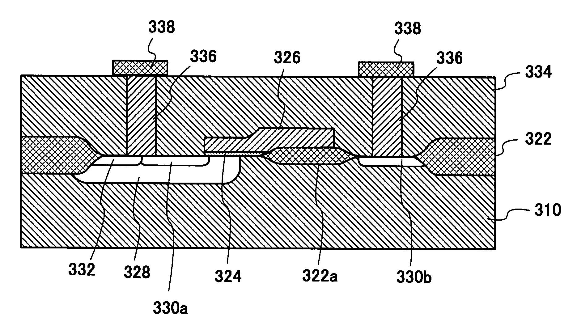
[0075]A semiconductor device according to a third embodiment of the present invention has a gate field plate structure in the same manner as the first and second embodiments mentioned above. As explained later herein, a silicone oxide film on which a part of a gate electrode lies is formed by the LOCOS oxidizing method, but the film thickness thereof is thinner than that of other field oxide film for isolation. For this reason, the flatness of the silicon substrate surface is maintained well in comparison with the conventional art structure. Furthermore, it is characterized by that the inclination of the end of the silicone oxide film (protective insulation film) is moderate, and the oxide film thickness under the gate electrode does not change sharply.

[0076]FIGS. 3A-3I are cross sectional views each showing a method of manufacturing a LDMOS (lateral diffused MOS) to become a semiconductor device according to the third embodiment of the present invention.

[0077]First, as shown in FIG...


PUM


Abstract

According to the present invention, there is provided a semiconductor device having a gate field plate structure, which includes a semiconductor substrate; a gate insulation film formed on the semiconductor substrate; a protective insulation film formed on the semiconductor substrate; a gate electrode formed on the gate insulation film; and a field plate electrode of the same electric potential as that of the gate electrode, formed on the protective insulation film. The protective insulation film is formed on the surface of the semiconductor substrate, and is not formed inside the substrate.

Description

CROSS REFERENCE TO RELATED APPLICATION[0001]This application claims the priority of Application No. 2006-262373, filed Sep. 27, 2006 in Japan, the subject matter of which is incorporated herein by reference.TECHNICAL FIELD OF THE INVENTION[0002]The present invention relates to a semiconductor device which employs a gate field plate structure, and a method of manufacturing the same.BACKGROUND OF THE INVENTION[0003]In a MOS (Metal-Oxide Semiconductor) device, as a means to secure the withstand voltage between source and drain, a gate field plate structure is employed, for example as shown in the following Non Patent Document 1. The gate field plate structure is formed so that the end of a gate electrode lies on a field oxide film formed usually by the LOCOS method, thereby distributing the electric field at the moment of gate-off and securing the withstand voltage. In general, it is applied to a lateral MOS device having withstand voltage approximately over 20V.[Non Patent Document 1]...

Claims


Application Information

Patent Timeline
Patent Type & Authority Applications(United States)
IPC IPC(8): H01L29/00H01L21/3205
CPCH01L21/32H01L29/7816H01L29/66681H01L29/42368
Inventor TANAKA, HIROYUKI
Owner LAPIS SEMICON CO LTD
Why Eureka
Try Eureka