Dielectric layers and methods of forming the same

a dielectric layer and dielectric layer technology, applied in the direction of basic electric elements, solid-state devices, electric apparatus, etc., can solve the problems of increasing the required capacitance per unit of footprint, complex fabrication steps, and increasing the processing cost. , to achieve the effect of reducing the average of leakage curren

Inactive Publication Date: 2008-04-24
ASM INTERNATIONAL
View PDF5 Cites 8 Cited by
  • Summary
  • Abstract
  • Description
  • Claims
  • Application Information

AI Technical Summary

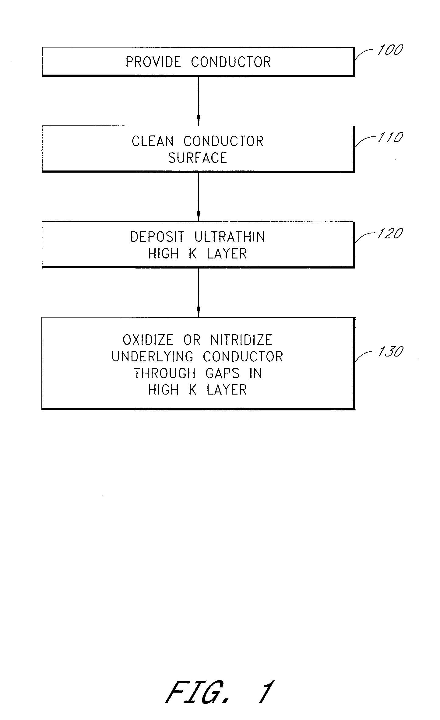
Problems solved by technology

As the chip area or “footprint” available per memory cell shrinks with each progressive generation of integrated circuits, the required capacitance per unit of footprint has increased.
Often, these structures require extremely complex fabrication steps, increasing the cost of processing significantly.
Such high defect densities lead to leakage currents through the dielectric and rapid device breakdown unacceptable for circuit designs with less than 0.25 μm gate spacing, i.e., sub-quarter-micron technology.
Moreover, even if the integrity of the silicon oxide is perfectly maintained, quantum-mechanical effects set fundamental limits on the scaling of silicon oxide.
However, silicon nitride has been found to exhibit a higher density of defects, such as interface trapping states, as compared to oxides.
The benefits of gate dielectrics made from silicon nitride are limited, however, because of the marginal increase in dielectric constant afforded by silicon nitride, particularly when used in conjunction with silicon oxide.
Several factors have limited the integration of such materials into current process flows, including the relative instability of high-k materials, a tendency to exhibit high defect densities, leakage currents, and the difficulty of avoiding oxidation of surrounding materials during high-k dielectric deposition and annealing.
Relatively complex process flows, however, are required to achieve such structures, and the overall dielectric constant of multiple-layer dielectric structures dilutes the effect of the high-k materials.

Method used


Image

  • Dielectric layers and methods of forming the same
  • Dielectric layers and methods of forming the same
  • Dielectric layers and methods of forming the same

Examples


example 1

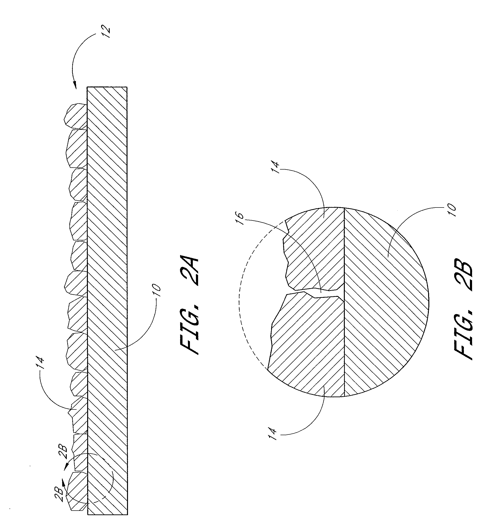
[0060] In this example, a high-k dielectric layer is formed on a silicon substrate by ALD. The skilled artisan will appreciate, however, that the high-k dielectric material can be formed by any suitable method (e.g., MOCVD).

[0061] Zirconium dioxide (ZrO2) was deposited by ALD onto a silicon substrate as follows. In pulse A, ZrCl4 vapor was introduced to the reaction chamber, exposing the wafer surface for 1.5 s. In purge A, the reaction chamber was purged with nitrogen gas for 3.0 s to remove excess ZrCl4 and reaction byproducts. Pulse A and purge A are together referred to as the “metal phase.” In pulse B, water vapor was introduced to the reaction chamber, exposing the wafer surface for 3.0 s. In purge B, residual H2O and reaction byproducts were removed by purging the reaction chamber with nitrogen gas for 4.0 s. Pulse B and purge B are together also referred to as the “oxygen phase.” During each of the reaction phases, the reactants were supplied in sufficient quantities to sat...

example 2

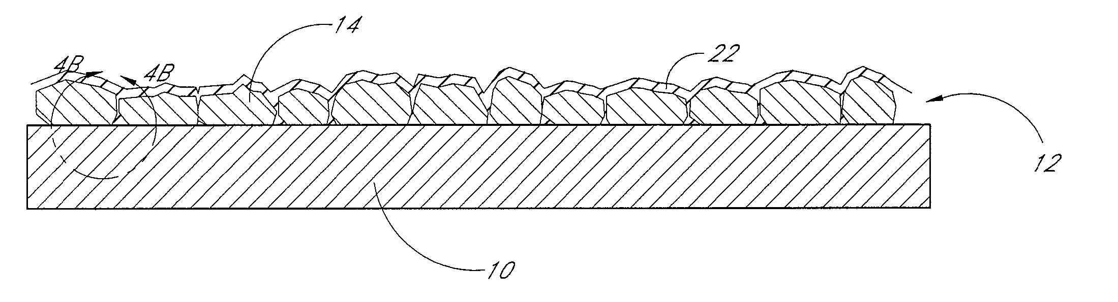
[0069]FIGS. 6-9 illustrate experimental results of oxidation and nitridation anneals of 4.0 nm ALD Al2O3 or HfO2 layers on 0.5 nm RTO (rapid thermal oxide) SiO2, an interfacial layer (24 in FIG. 5A). Anneals were performed at from 600° C. to 1000° C. for 60 s. The wafers were then annealed at 400° C. under forming gas before measurement of an EOT parameter. This second anneal does not affect the interface oxide. In these examples, an EOT parameter was measured using a Corona-Oxide-Si (COS) method on a COS Quantox system (KLA-Tencor Corp.). The EOT parameter (GateTox™) is the accumulation capacitance, expressed in Å.

[0070]FIG. 6 illustrates the EOT of Al2O3 dielectric layers under a series of oxidation annealing conditions. The EOT increased under higher oxygen concentrations (40 Torr and 3×10⁻² Torr) at higher temperatures. The Al2O3 high-k layer was stable up to from about 900° C. to about 1000° C. under sufficient oxygen concentrations. EOT decreased in lean oxygen anneals. The E...


PUM

PropertyMeasurementUnit
thicknessaaaaaaaaaa
thicknessaaaaaaaaaa
thicknessaaaaaaaaaa

Abstract

High dielectric constant (high-k) materials are formed directly over oxidation-susceptible conductors such as silicon. A discontinuous layer is formed, with gaps between grains of the high-k material. Exposed conductor underneath the grain boundaries is oxidized or nitridized to form, e.g., silicon dioxide or silicon nitride, when exposed to oxygen or nitrogen source gases at elevated temperatures. This dielectric growth is preferential underneath the grain boundaries such that any oxidation or nitridation at the interface between the high-k material grains and covered conductor is not as extensive. The overall dielectric constant of the composite film is high, while leakage current paths between grains is reduced. Ultrathin high-k materials with low leakage current are thereby enabled.

Description

REFERENCE TO RELATED APPLICATION [0001] The present application is a divisional of U.S. application Ser. No. 10 / 379,516, filed Mar. 4, 2003 and claims the priority benefit under 35 U.S.C. §119(e) to U.S. provisional application No. 60 / 362,249, filed Mar. 5, 2002.FIELD OF THE INVENTION [0002] The present invention relates generally to the manufacturing of integrated circuits, and more particularly to the preparation of high-k dielectric layers in integrated circuits. BACKGROUND OF THE INVENTION [0003] Process control is very important in the fabrication of ultra-large scale integrated circuits. Through a series of deposition, doping, photolithography and etch steps, the starting substrate and subsequent layers are converted into integrated circuits, with a single substrate producing from tens to thousands or even millions of integrated devices, depending on the size of the wafer and the complexity of the circuits. [0004] One area in which process control is particularly critical is t...

Claims


Application Information

Patent Timeline
Patent Type & Authority Applications(United States)
IPC IPC(8): H01L23/58H01L21/02
CPCH01L28/56H01L28/60H01L2924/0002H01L2924/00
Inventor RAAIJMAKERS, IVOSOININEN, PEKKA J.MAES, JAN WILLEM
Owner ASM INTERNATIONAL
Why Eureka
Try Eureka