Semiconductor memory, system, testing method for system

a memory and semiconductor technology, applied in the field of system testing technology, can solve the problems of reducing test efficiency, difficult for the manufacturer to distribute logic data, and complicated test patterns for memory chips, so as to reduce the test cost of a system

Inactive Publication Date: 2008-05-01
FUJITSU MICROELECTRONICS LTD
View PDF9 Cites 14 Cited by
  • Summary
  • Abstract
  • Description
  • Claims
  • Application Information

AI Technical Summary

Benefits of technology

[0012] An object of the present invention is to reduce test costs of a system in which a plurality of types of memory chips is mounted in one package.
[0013] In an aspect of the present invention, a test pattern generator of a semiconductor memory (first memory chip) generates a plurality of test patterns. Test patterns are output from a plurality of external output terminals of the first memory chip to test a different type of memory chip (second memory chip) mounted in the same package as the first memory chip. Then, not only a memory cell array of the first memory chip, but also the second memory chip is tested by the test patterns. Therefore, if different types of memory chips are mounted in the same package and even when no terminal of the memory chip is connected to an external terminal of a system, the memory chip can be tested. Since the system does not need to form a useless external terminal, system costs can be reduced. Also, since no testing apparatus to generate complicated test patterns is needed, test costs can be reduced.
[0014] In contrast to programmable logic, a test pattern generator is configured using nonvolatile logic. Thus, there is no need to read circuit data of the test pattern generator before a test. Since a test can be carried out without preparing test patterns in advance, a user who purchases the first and second memory chips to configure a system can also carry out a test easily. That is, test costs can be reduced.

Problems solved by technology

Test patterns to test memory chips are generally complicated and it is necessary to use an LSI tester (memory tester) for memory to test memory chips.
In this case, the user must purchase an expensive LSI tester.
If the user should have both the memory tester and logic tester, tests must be performed by alternately setting the MCP or SiP to the memory tester and logic tester, decreasing test efficiency.
However, it is difficult for the manufacturer to distribute logic data to all users who assemble a system such as an MCP and SiP in view of time and costs.
Moreover, since logic data needs to be written to programmable logic each time a test is carried out, the test time and test costs of a system increase.
Therefore, it is not realistic to test a system such as an MCP and SiP using programmable logic in the memory chip.

Method used


Image

  • Semiconductor memory, system, testing method for system
  • Semiconductor memory, system, testing method for system
  • Semiconductor memory, system, testing method for system

Examples


first embodiment

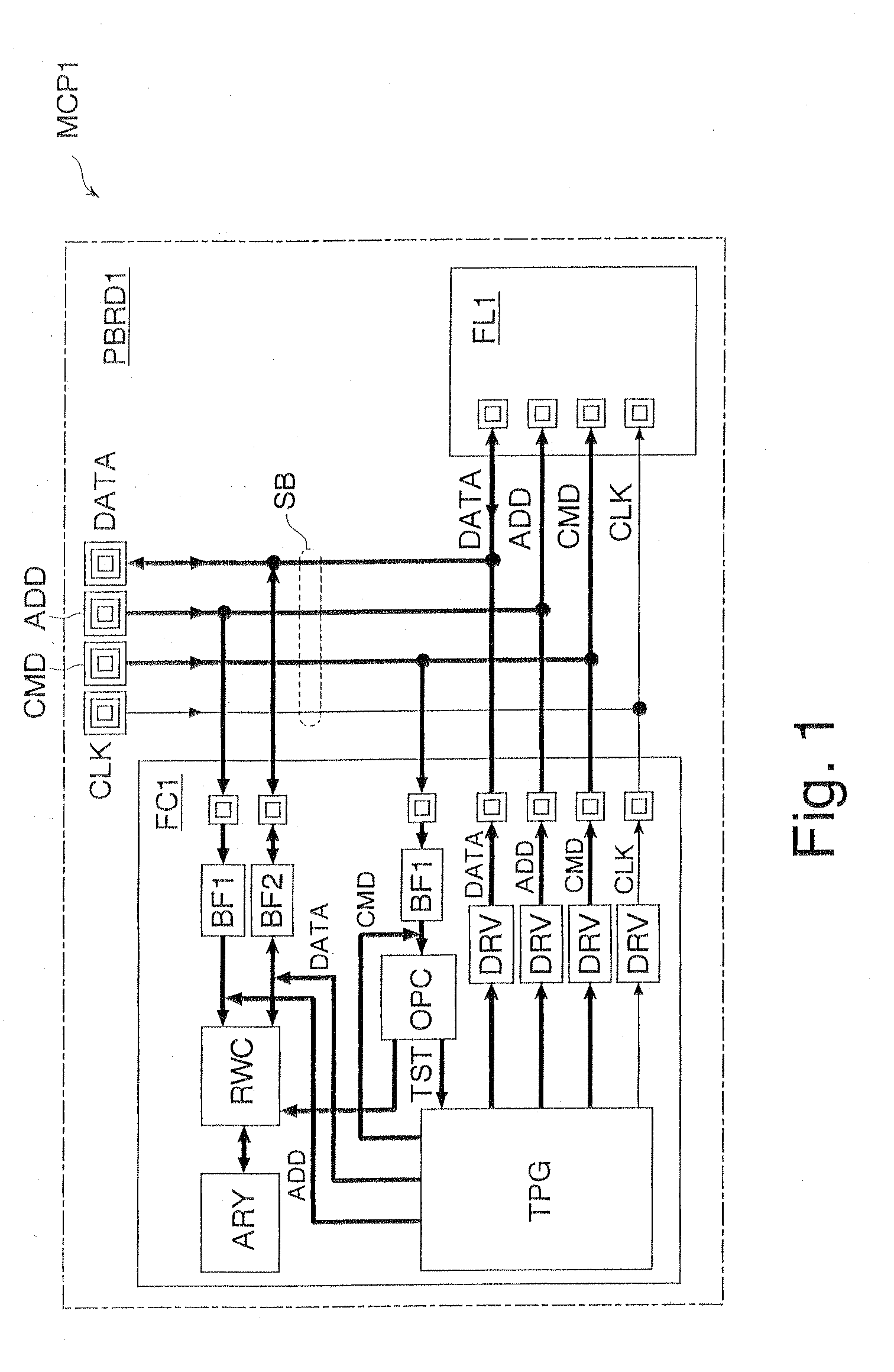
[0039]FIG. 1 shows a In this embodiment, an FCRAM chip FC1 (Fast Cycle RAM: first memory chip) and a flash memory chip FL1 (second memory chip) are mounted on a package board PBRD1 to form a multi-chip package MCP1 (system). The MCP1 is mounted, for example, in portable equipment such as a mobile phone. The FCRAM chip FC1 has a DRAM memory core and is a kind of pseudo SRAM chip having an SRAM interface. The FCRAM chip FC1 operates asynchronously with a clock and the flash memory chip FL1 operates synchronously with a clock. The FCRAM chip FC1 and the flash memory chip FL1 are also called a chip FC1 and a chip FL1 respectively below.

[0040] The chip FC1 has a memory cell array ARY having volatile memory cells (dynamic memory cells), a read / write control circuit RWC, a plurality of buffers BF1 and BF2, an operation control circuit OPC, a test pattern generator TPG, a plurality of drivers DRV, and a plurality of pads. The read / write control circuit RWC receives during write operation a...
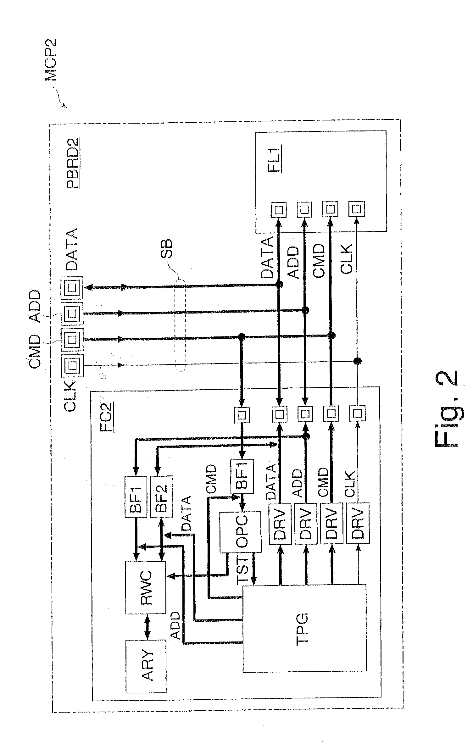
second embodiment

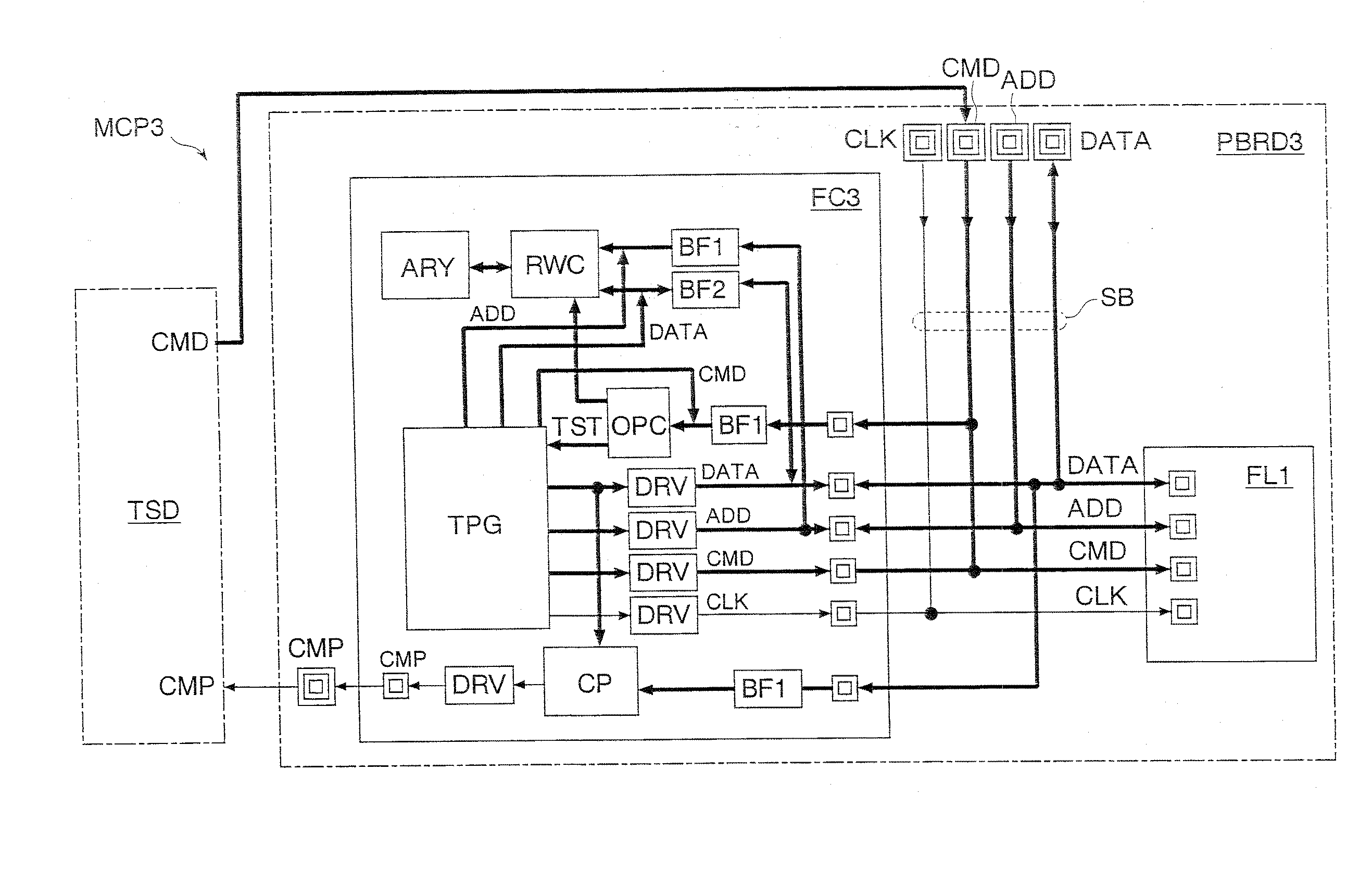
[0057] The chip FC3 has, in addition to the configuration of the chip FC2 in the second embodiment, pads (external input terminals) connected successively, the buffer BF1, a comparator CP, the driver DRV, and the test result terminal CMP (pad). The comparator CP compares test write data for the chip FL1 output from the test pattern generator TPG and test read data read from the chip FL1 into which the test write data has been written via the buffer BF1, and outputs a comparison result to the test result terminal CMP via the driver DRV. The test result terminal CMP is a dedicated terminal for outputting a test result signal CMP indicating the test result.

[0058] The package board PBRD3 is the same as the package board PBRD2 in the second embodiment except that pattern wiring and connection specifications (bonding specifications) are different to connect a data line DATA of the system bus SB to a pad corresponding to the comparator CP and a test result terminal CMP (a system-test conne...

third embodiment

[0061] Also in the third embodiment, as described above, an effect similar to that of the above embodiments can be obtained. Further, the test result terminal CMP is formed on the chip FC3 and the package board PBRD3 in the present embodiment and therefore, the testing apparatus TSD can determine whether the MCP3 is a good product or a bad one based solely on a test result transmitted to the test result terminal CMP without reading data from the chips FC1 and FL1. Thus, the testing apparatus TSD can be configured by a simple circuit. As a result, test costs can be reduced.

[0062] Further, also when many MCP3's are mounted on the evaluation board, signals required for the testing apparatus TSD are only the test command signal CMD common to a plurality of MCP3's and the test result signal CMP required for each MCP3. Many MCP3's can be tested at a time due to the simple testing apparatus TSD and therefore, the test time and test costs can significantly be reduced.


PUM


Abstract

A plurality of test patterns generated by a test pattern generator is output from a first memory chip to test a second memory chip, which is of a different type from the first memory chip and mounted in the same package. Therefore, when different types of memory chips are mounted in the same package, the memory chip is tested even no terminal of the memory chip is connected to an external terminal of a system. Since there is no need to form any useless terminal in the system, system cost is reduced. Since a testing apparatus generating complicated test patterns is made unnecessary, test cost is reduced. The test pattern generator is constructed using nonvolatile logic and therefore, tests can be carried out without preparing test patterns in advance. Consequently, a user who purchases the first and second memory chips to construct a system can also carry out tests easily.

Description

CROSS-REFERENCE TO RELATED APPLICATION [0001] This application is a Continuation Application of International Application No. PCT / JP2005 / 007646, filed Apr. 21, 2005, designating the U.S.BACKGROUND [0002] 1. Field [0003] The present invention relates to a testing technology for a system configured by mounting a plurality of types of semiconductor memory chips in one package. [0004] 2. Description of the Related Art [0005] In recent years, a technology called SiP (System in Package) or MCP (multi-chip package) to configure a system by housing a plurality of types of memory chips and logic chips whose processing technologies are different from each other in one package has been developed. Also, a technology called SoC (System on chip) to configure a system by integrating a plurality of types of memory circuits and logic circuits on one chip has been developed. [0006] In such types of system (for example, SiP), an external terminal is formed for signals that need to be input / output from...

Claims


Application Information

Patent Timeline
Patent Type & Authority Applications(United States)
IPC IPC(8): G06F11/277
CPCG11C29/36G11C2029/3602G11C2029/0401G11C29/00
Inventor UCHIDA, TOSHIYA
Owner FUJITSU MICROELECTRONICS LTD
Why Eureka
Try Eureka