Method of Correcting Photomask Defect

a technology of photomask and defect, applied in the field of photomask defect correction, can solve the problems of image damage (decrease in transmittance) of glass parts, insufficient resolution power, and inability to correct fine patterns in most tips, etc., to avoid charge-up, high accuracy, and good quality

Inactive Publication Date: 2008-05-08
SII NANOTECHNOLOGY INC
View PDF2 Cites 6 Cited by
  • Summary
  • Abstract
  • Description
  • Claims
  • Application Information

AI Technical Summary

Benefits of technology

[0009] Since it is possible to avoid the charge-up by an excessive electric charge accumulation if also the isolated pattern can be connected to other pattern by the conductor wire, it is possible to perform a working of a high accuracy, in which an image is good in its quality and there is no drift, by a charge, of the electron beam or the helium ion beam generating from the gas field ion source. Further, the gas assist etching of the electron beam or the helium ion beam generating from the gas field ion source has a material dependency and, although there exists also a material not capable of being shaved, any material can be shaved off if the AFM scratch working is used.
[0010] Even in the case where the suitable longitudinal and lateral pattern for the drift correction does not exist in the working window, it is possible to use the metal deposition film provided by the CVD, in which the electron beam or the helium ion beam generating from the gas field ion source is used, as the drift marker. Since the charge-up can be avoided by the fact that the metal deposition film becomes the conductor wire, it is possible to take the image, in which there is no drift by the charge as well and whose quality is good, of the drift marker. By the drift correction using the image whose quality is good, since the drift in a working position of the electron beam or the helium ion beam generating from the gas field ion source can be highly accurately corrected, it is possible to perform a highly accurate working.

Problems solved by technology

However, with the laser, a resolving power is insufficient and thus the defect of a fine pattern in a most tip cannot be corrected and, with the focused ion beam, an imaging damage (decrease in transmittance) of a glass part, which is due to an implantation of gallium used as a primary beam, becomes an issue following upon the shortening of the wavelength of the light source of the reduced projection exposure apparatus.
Further, there is known the fact that the imaging damage is not exerted even if a rare gas ion beam is used, besides the electron beam.
However, since the photomask is one in which a metal film is deposited on a glass in order to shield a light, in a case where an area of a metal film pattern is small, a charge-up generates by an excessive electric charge in an electron beam irradiation.
If the charge-up occurs, there are a decrease in a quality of a secondary electron image, and an issue that a drift of the electron beam generates, thereby decreasing a working accuracy.
Further, hitherto, although a fine hole or protrusion is made by the electron beam and it is utilized as a drift marker, it is becoming difficult to provide the hole or protrusion like this in order to fine the pattern and shorten an exposure wavelength.

Method used


Image

  • Method of Correcting Photomask Defect
  • Method of Correcting Photomask Defect
  • Method of Correcting Photomask Defect

Examples


Embodiment Construction

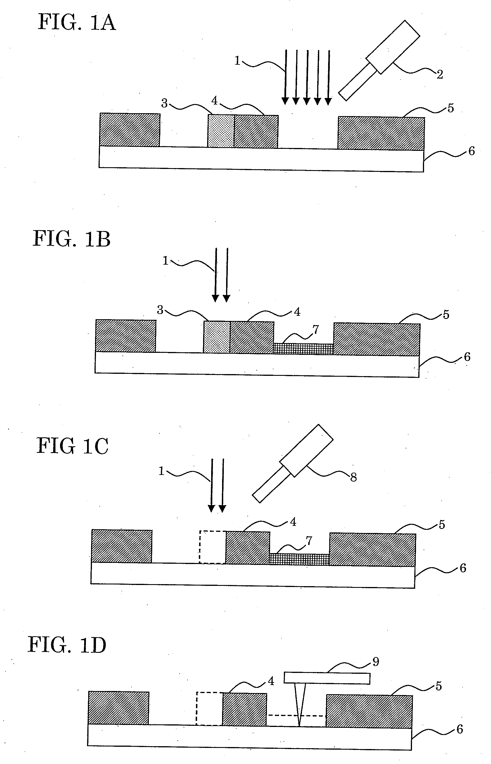
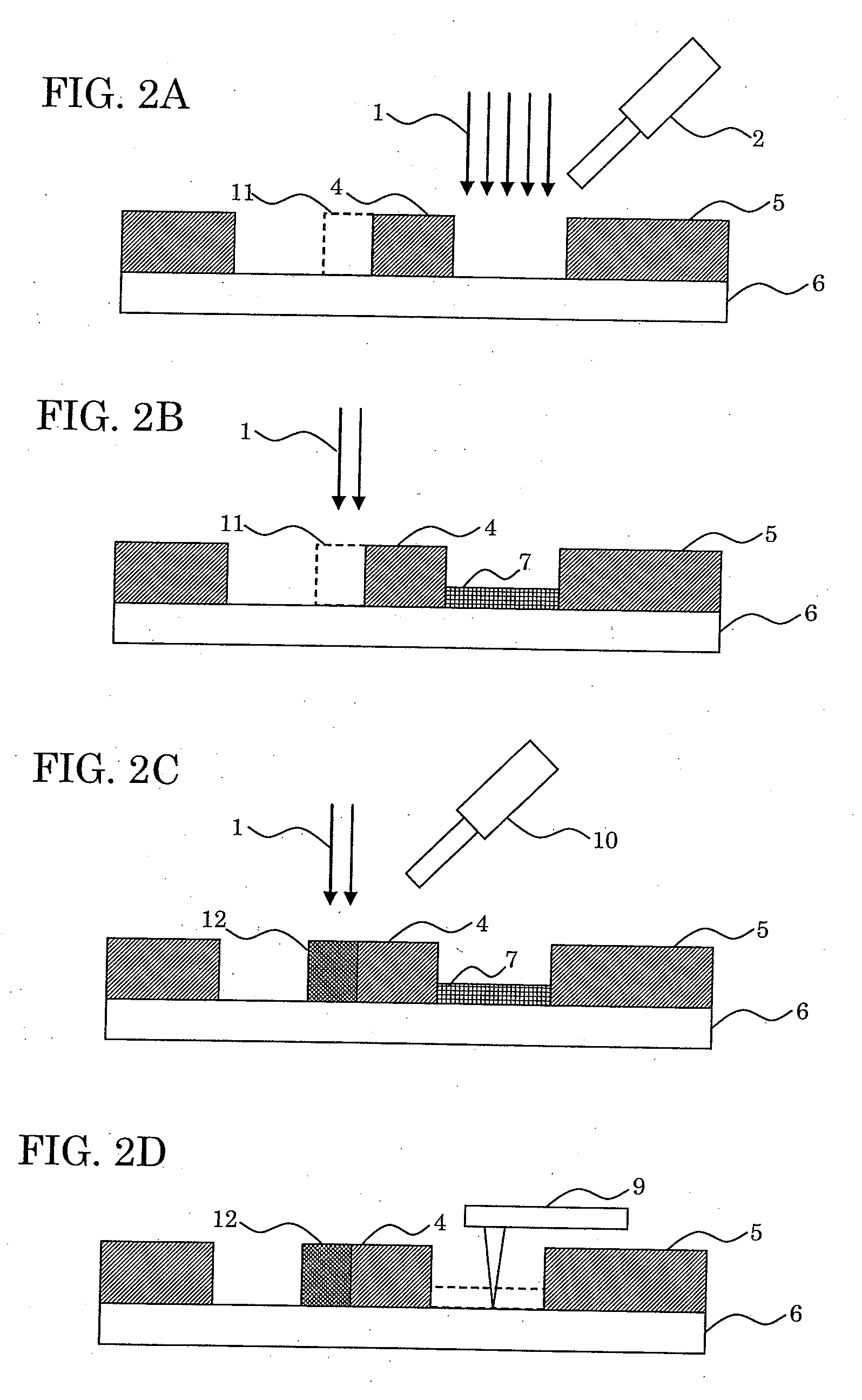
[0015] Hereunder, about an embodiment of the present invention, there is detailedly explained by using the drawings. FIGS. 1A-1D are schematic sectional views of the photomask, for explaining a case correcting the opaque defect of the isolated pattern by the present invention, and FIGS. 2A-2D are schematic sectional views of the photomask, for explaining a case correcting the clear defect of the isolated pattern by the present invention.

[0016] The photomask having the defect is introduced to an electron beam fine working apparatus having a shading film raw material gas introduction system 10, a metal deposition film raw material gas introduction system 2, and a gas introduction system 8 for a gas assist etching, and an XY stage is moved such that a defect position previously found by a defect inspection device enters into a visual field.

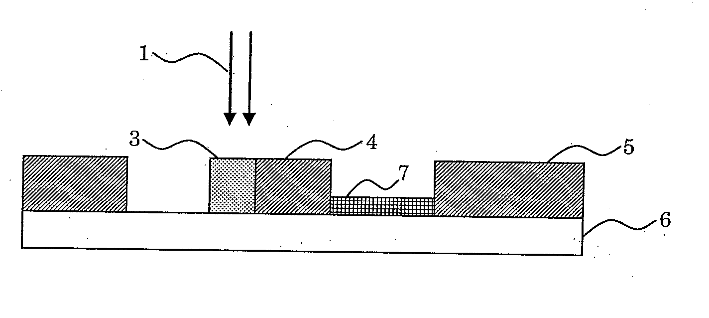
[0017] A region including the defect is observed and, in a case where an isolated defect or an isolated pattern 4 on a glass substrate 6, in which...


PUM

PropertyMeasurementUnit
sizeaaaaaaaaaa
AFMaaaaaaaaaa
defectaaaaaaaaaa

Abstract

After making an electrical continuity in the isolated pattern by a metal deposition film by a CVD of the electron beam or the helium ion beam generating from the gas field ion source, the defect is corrected and, after the correction, the metal deposition film is physically removed by an AFM scratch working probe. A worked waste generated by the AFM scratch working is removed by a washing.

Description

RELATED APPLICATIONS [0001] This application claims priority under 35 U.S.C. §119 to Japanese Patent Application Nos. JP2006-295836 filed Oct. 31, 2006, and JP2007-220474 filed Aug. 28, 2007, the entire content of which is hereby incorporated by reference. BACKGROUND OF THE INVENTION [0002] The present invention is one relating to a method of correcting a defect in an isolated pattern of a photomask, in which there is used an electron beam or a helium ion beam from a gas field ion source. [0003] A lithography responds to a demand for fining a semiconductor integrated circuit by shortening a wavelength of a light source of a reduced projection exposure apparatus and increasing an NA. A defect correction of the photomask, in which there is demanded the fact that there is no defect in an original form of a transcription in the reduced projection exposure apparatus, is performed hitherto by using a laser or a focused ion beam. However, with the laser, a resolving power is insufficient a...

Claims


Application Information

Patent Timeline
Patent Type & Authority Applications(United States)
IPC IPC(8): G03F1/00G03F1/08G03F1/72G03F1/74
CPCG03F1/72G03F1/74
Inventor TAKAOKA, OSAMUTASHIRO, JUNICHI
Owner SII NANOTECHNOLOGY INC
Why Eureka
Try Eureka