Nitride semiconductor laser diode

a laser diode and semiconductor technology, applied in semiconductor lasers, laser details, electrical equipment, etc., can solve the problems high substrate cost, and limit the reduction of the cost of gan-based semiconductor laser diodes, so as to reduce the number of crystal defects, the effect of improving the reliability and reducing the cos

Inactive Publication Date: 2008-05-15
PANASONIC CORP
View PDF9 Cites 40 Cited by
  • Summary
  • Abstract
  • Description
  • Claims
  • Application Information

AI Technical Summary

Benefits of technology

[0050] With this configuration, the nitride semiconductor is grown in a lateral direction on the mask film, so that a portion grown in the lateral direction on the mask film in the nitride semiconductor has less number of crystal defects. Hence, a blue-violet semiconductor laser diode with higher performance and higher reliability can be realized.
[0051] As described above, according to the nitride semiconductor laser diode in accordance with the present invention, the cleaved facet which is composed of the highly reflective facet mirror can be formed in the nitride semiconductor laminate and formed on the silicon substrate of which principal surface is the {100} plane. Thus, although the nitride semiconductor laser diode is manufactured on an inexpensive silicon substrate, the nitride semiconductor laser diode can realize a low threshold current and a low operating current. The cost of the blue-violet semiconductor laser can be reduced with the above high performance maintained.

Problems solved by technology

However, a currently available GaN substrate is manufactured by thick film growth by a hydride vapor phase epitaxy (HVPE) method instead of a conventional bulk growth forming a boule, so that there is a limitation to increase in the throughput and wafer size keeping good crystal quality.
For this reason, the cost of the substrate tends to be high and hence there would be a limitation to reduction in cost of the GaN-based semiconductor laser diode.
Thus, there arises a problem that a cleavage face perpendicular to the principal surface of a laser structure on a Si(111) cannot be obtained.
Thus, when considering the relationship of a crystal orientation between the Si substrate and the GaN-based semiconductor epitaxially grown on the Si substrate, the cleavage facet of the laser structure in Patent Document 1 does not match with the one of the Si substrate, so a good cleavage facet cannot be obtained.
As a result, it is very difficult to achieve low enough threshold current and operating current which are required for the practical use.

Method used


Image

  • Nitride semiconductor laser diode
  • Nitride semiconductor laser diode
  • Nitride semiconductor laser diode

Examples


first embodiment

[0059] A first embodiment of the present invention will be described with reference to the drawings.

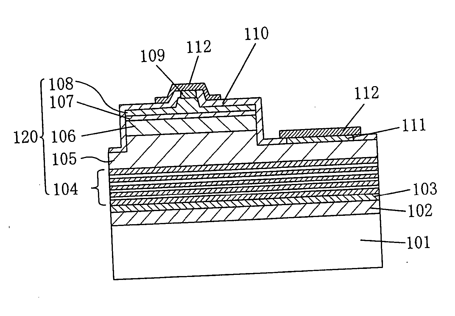
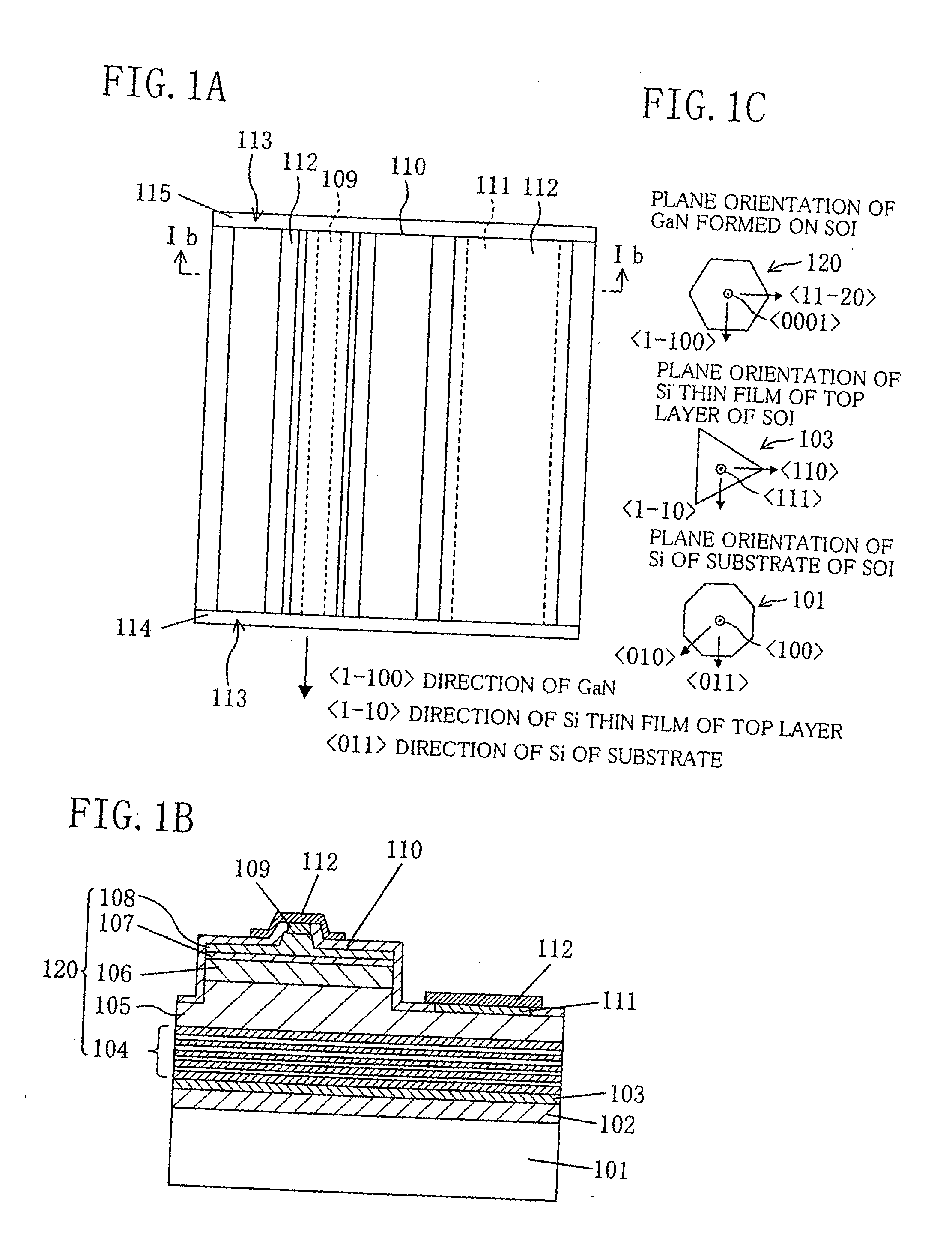
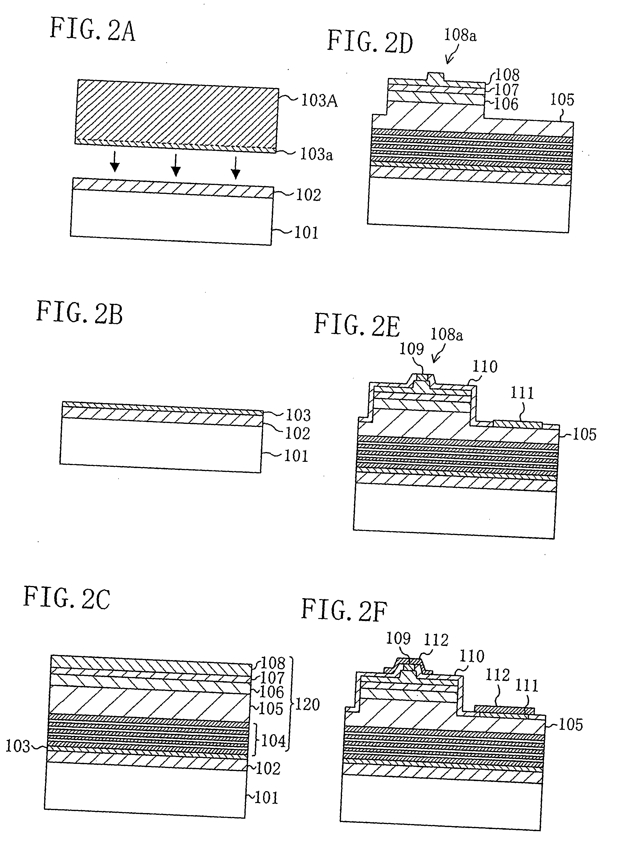
[0060]FIG. 1A and FIG. 1B show a nitride semiconductor laser diode according to the first embodiment of the present invention. FIG. 1A is a plan construction and FIG. 1B is a section construction along a line Ib-Ib in FIG. 1A.

[0061] As shown in FIG. 1A and FIG. 1B, the nitride semiconductor laser diode according to the first embodiment of the present invention includes: a so-called SOI (Silicon-On-Insulator) substrate including a substrate 101 made of silicon (Si) of which principal surface is a {100} plane; an insulating film 102 formed of silicon oxide (SiO2) on the substrate 101 in a film thickness of about 100 nm, and a thin film 103 formed on the insulating film 102, having a film thickness of about 10 nm, and made of Si of which principal surface is a {111} plane; and a nitride semiconductor 120 including plural nitride semiconductor layers which are formed on the SOI substrat...

second embodiment

[0093] A second embodiment of the present invention will be described below with reference to the drawings.

[0094]FIGS. 4A and 4B show a nitride semiconductor laser diode in accordance with the second embodiment of the present invention. FIG. 4A shows a plan structure and FIG. 4B shows a cross sectional structure along a line IVb-IVb in FIG. 4A.

[0095] As shown in FIG. 4B, in the nitride semiconductor laser diode in accordance with the second embodiment, indented and projected portions 201a made of plural facets of {111} planes are formed on the principal surface of a n-type silicon substrate 201 of which plane orientation is a {100} plane, and a nitride semiconductor 220 is formed on the indented and projected portions 201a to form a blue-violet semiconductor laser diode.

[0096] Further, as shown in FIG. 4C, the {011} plane of the cleaved facet of the substrate 201 is formed so as to be parallel to the {1-100} plane of the cleaved facet of the nitride semiconductor 220.

[0097] Spec...


PUM


Abstract

A nitride semiconductor laser diode includes: a substrate made of silicon in which a plane orientation of a principal surface is a {100} plane; and a semiconductor that includes a plurality of semiconductor layers formed on the substrate and including an active layer, each of the plurality of semiconductor layers being made of group III nitride. The semiconductor has a plane parallel to a {011} plane which is a plane orientation of silicon as a cleaved facet, the cleaved facet forming a facet mirror.

Description

CROSS REFERENCE TO RELATED APPLICATIONS [0001] This non-provisional application claims priority under 35 U.S.C. §119(a) on Patent Application No. 2006-304139 filed in Japan on Nov. 9, 2006, the entire contents of which are hereby incorporated by reference. BACKGROUND OF THE INVENTION [0002] 1. Field of the Invention [0003] The present invention relates to a nitride semiconductor laser device applicable to a blue-violet semiconductor laser device used for a light source for writing and reading a high-density optical disk. [0004] 2. Description of Related Art [0005] A group III-V nitride compound semiconductor (generally expressed by InGaAlN) typified by gallium nitride (GaN) is a material having a wide bandgap (in the case of GaN, 3.4 eV at room temperature) and capable of realizing an optoelectronic devices emitting the wavelength ranging from green to ultra-violet. Blue / green light emitting diodes have been commercialized and widely used in various displays and indicators. Moreover...

Claims


Application Information

Patent Timeline
Patent Type & Authority Applications(United States)
IPC IPC(8): H01S5/323
CPCH01S5/021H01S5/32341H01S5/2201
Inventor UEDA, TETSUZOUEDA, DAISUKE
Owner PANASONIC CORP
Why Eureka
Try Eureka