Method for Manufacturing Silicon Wafer and Silicon Wafer Manufactured by this Method

a manufacturing method and technology for silicon wafers, applied in the direction of silicon compounds, semiconductor/solid-state device testing/measurement, instruments, etc., can solve the problems of easy deformation of wafers, and reduced device yield ratio, etc., to achieve high yield ratio, low cost, and short time

Active Publication Date: 2008-05-22
SUMCO CORP
View PDF4 Cites 13 Cited by
  • Summary
  • Abstract
  • Description
  • Claims
  • Application Information

AI Technical Summary

Benefits of technology

[0019]As described above, according to the present invention, first, by inputting as input parameters respective combinations of the plurality of types of oxygen concentrations and thermal histories which are set to manufacture the silicon wafer, the Fokker-Planck equation is solved to calculate each of the diagonal length L and the density D of the oxygen precipitates in the wafer after the heat treatment step of forming the oxygen precipitates and immediately before the heat treatment step of the device manufacturing process, then the maximum heat treatment S acting in the tangent line direction of the outer peripheral portion of the wafer in the heat treatment step of the device manufacturing process is calculated based on the structure and the heat treatment temperature of the heat treatment furnace used in the heat treatment step of the device manufacturing process, the oxygen concentration and others satisfying the relationship of Expression (1) are subsequently determined, and hence, even if a dia...

Problems solved by technology

Therefore, in the state-of-the-art process using a wafer having a diameter of 300 mm, a slip is apt to occur easil...

Method used


Image

  • Method for Manufacturing Silicon Wafer and Silicon Wafer Manufactured by this Method
  • Method for Manufacturing Silicon Wafer and Silicon Wafer Manufactured by this Method
  • Method for Manufacturing Silicon Wafer and Silicon Wafer Manufactured by this Method

Examples


first embodiment

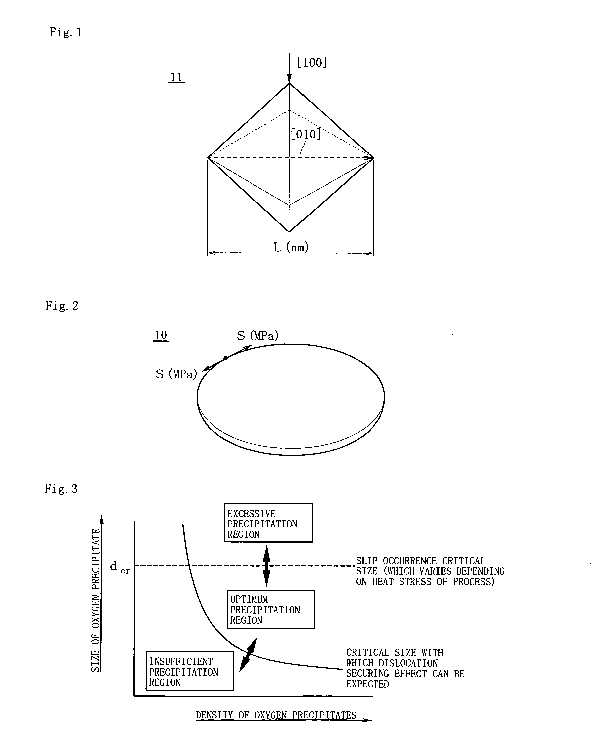
[0033]As shown in FIGS. 1 and 2, a silicon wafer 10 is a silicon wafer obtained by slicing a silicon single-crystal rod grown based on the CZ method, to which a heat treatment is then applied to form oxygen precipitates 11 inside and of which at least a main surface is subjected to mirror polishing processing. This wafer 10 is then shipped to a semiconductor device manufacturer and subjected to a heat treatment in a device manufacturing process.

[0034]On the other hand, FIG. 3 is a schematic view showing a concept of a relationship between a density and a diagonal length (a size) of oxygen precipitates formed in the wafer after the heat treatment step of forming the oxygen precipitates and immediately before the heat treatment step of the device manufacturing process, where there are lower limit values of the diagonal length (the size) and the density of the oxygen precipitates within which a dislocation in the wafer can be secured even if a heat stress functions in the heat treatmen...

second embodiment

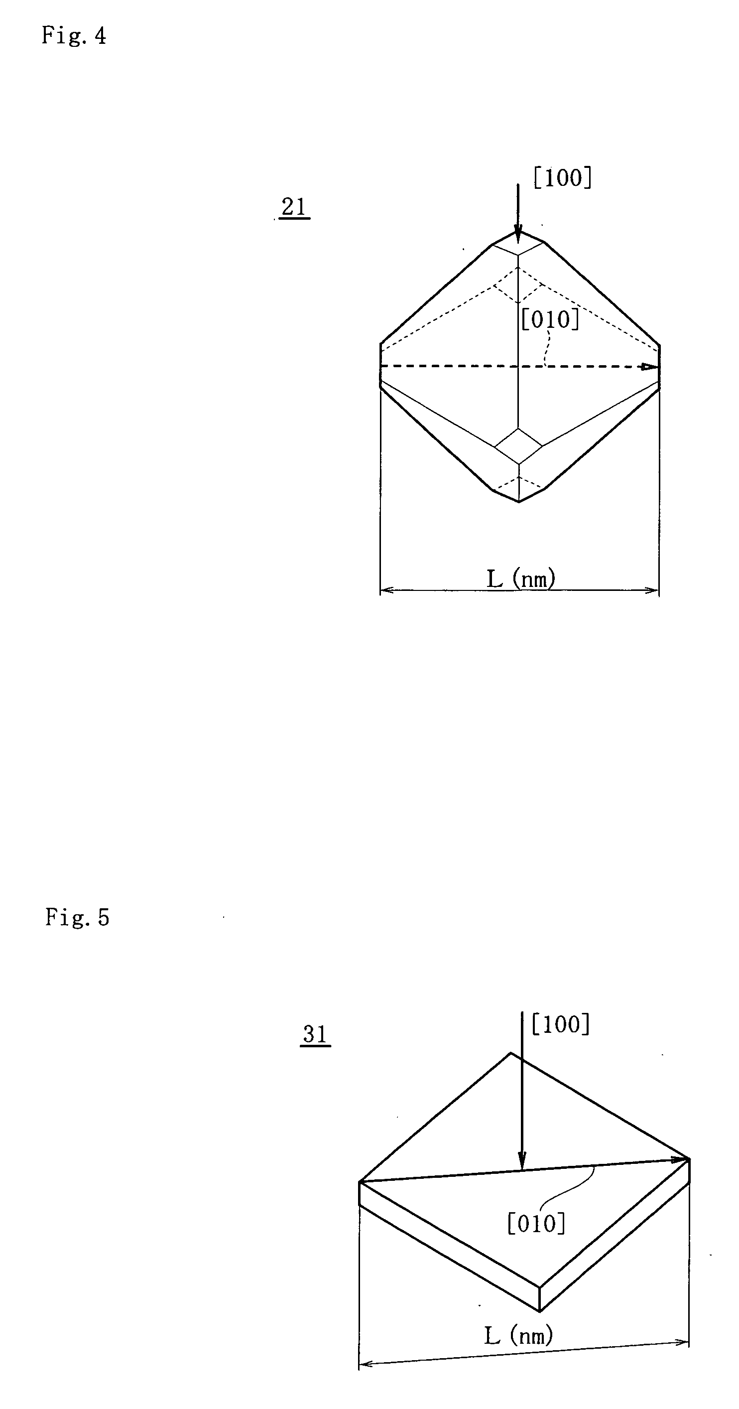
[0054]FIG. 4 shows a second embodiment according to the present invention.

[0055]In this example, a shape of an oxygen precipitate 21 formed in a silicon wafer is a 14-faceted shape. This 14-faceted oxygen precipitate 21 has a shape obtained by chamfering six corners of the regular octahedron oxygen precipitate in the first embodiment. The regular octahedron oxygen precipitate in the first embodiment and the 14-faceted oxygen precipitate 21 in this embodiment are generically called a polyhedral oxygen precipitate. Other structures are formed to be equal to those in the first embodiment. Moreover, in this example, a diagonal length (a size) of the oxygen precipitate 21 means a diagonal length extending in a crystal orientation direction [010] of the 14-faceted oxygen precipitate 21 when this oxygen precipitate 21 is seen from a crystal orientation direction [100] of a silicon wafer.

third embodiment

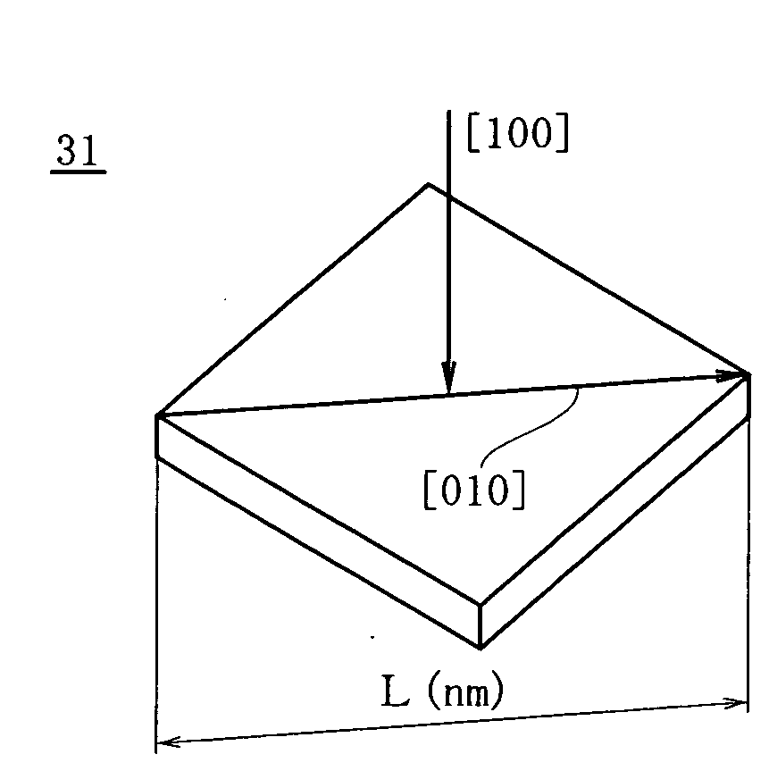
[0056]FIG. 5 shows a third embodiment according to the present invention.

[0057]In this embodiment, a shape of an oxygen precipitate 31 formed in a silicon wafer is a square tabular shape.

[0058]Additionally, assigning a size distribution function f(r,t) after an arbitrary heat treatment to Expression (5) mentioned above and the following Expression (7) can calculate a diagonal length L (nm) and a density (pieces / cm3) of an oxygen precipitate 11 (a square tabular oxygen precipitate).

[NumericalExpression4]L(nm)=107×[8β]1 / 3∫rf(r,t)r∫f(r,t)r=107×[8β]1 / 3∫rf(r,t)rD(7)

[0059]In Expression (7), β is an aspect ratio (a thickness / a diagonal length of the square tabular oxygen precipitate) of the oxygen precipitate (the square tabular oxygen precipitate) and it is a value of approximately 0.01. Other structures are formed to be equal to those in the first embodiment. Additionally, in this embodiment, the diagonal length (the size) of the oxygen precipitate 31 means a diagonal length extending in...


PUM


Abstract

There is obtained a silicon wafer which has a large diameter, where no slip generated therein in a wide range of a density of oxygen precipitates even though a heat treatment such as SLA or FLA is applied thereto, and which has high strength.
First, by inputting as input parameters combinations of a plurality of types of oxygen concentrations and thermal histories set for manufacture of a silicon wafer a Fokker-Planck equation is solved to calculate each of a diagonal length L and a density D of oxygen precipitates in the wafer after a heat treatment step to form the oxygen precipitates (11) and immediately before a heat treatment step of a device manufacturing process is calculated. Then, a maximum heat stress S acting in a tangent line direction of an outer peripheral portion of the wafer in the heat treatment step of the device manufacturing process is calculated based on a heat treatment furnace structure and a heat treatment temperature used in the heat treatment step of the device manufacturing process, and then an oxygen concentration or the like satisfying the following Expression (1) is determined:
12000×D−0.26≦L≦51000×S−1.55  (1)

Description

TECHNICAL FIELD[0001]The present invention relates to a method for manufacturing a silicon wafer in which oxygen precipitates are formed and no slip occurs, and a silicon wafer manufactured by this method.BACKGROUND ART[0002]A wafer cut out from a silicon single crystal obtained by a Czochralski method (which will be referred to as a CZ method hereinafter) has been conventionally used in order to manufacture a semiconductor device. In a device manufacturing process, a wafer undergoes various heat treatments and a slip may be produced in the wafer in some cases, but a regular batch type heat treatment furnace is used in a conventional process and a diameter of a wafer which is as small as 200 mm is primarily used, and hence occurrence of the slip is not a very serious problem.[0003]However, in a state-of-the-art device manufacturing process in recent years, a single-wafer processing type heat treatment method such as SLA (Spike Lamp Anneal) or FLA (Flash Lamp Anneal) is used as a hea...

Claims


Application Information

Patent Timeline
IPC IPC(8): H01L21/66C01B33/00
CPCC30B29/06H01L21/3226H01L21/3225C30B33/02
Inventor SADAMITSU, SHINSUKESUGIMURA, WATARUAKATSUKA, MASANORIHOURAI, MASATAKA
Owner SUMCO CORP
Why Eureka
Try Eureka