Method for manufacturing light-emitting diode, light-emitting diode, lightsource cell unit, light-emitting diode backlight, light-emitting diode illuminating device, light-emitting diode display, and electronic apparatus

Inactive Publication Date: 2008-05-29
SONY CORP
View PDF3 Cites 100 Cited by
  • Summary
  • Abstract
  • Description
  • Claims
  • Application Information

AI Technical Summary

Benefits of technology

[0072]According to the structures described above of the embodiments of the present invention, when the refractive index of the dielectric substance forming the convex portions is appropriately selected, the far-field pattern of the light-emitting diode can be controlled without using an optical component such as a lens, and when the refractive index is optimized, the light extraction efficiency and the light-scattering property can both be improved. In addition, since the growth of the first nitride-based III-V compound semiconductor layer is started from the bottom surface of the concave portion on the substrate, and the first nitride-based III-V compound semiconductor layer is grown through the state of the triangle cross-sectional shape using the bottom surface of the concave portion as the base, the concave portion can be filled without forming any spaces. Subsequently, from the first nitride-based III-V compound semiconductor layer thus grown, the second nitride-based III-V compound semiconductor layer is grown in the lateral direction. In this step, in the first nitride-based III-V compound semiconductor layer, dislocation is generated from the interface with the bottom surface of the concave portion on the substrate in a direction perpendicular to one major surface of the substrate and then extends to the inclined surface of the first nitride-based III-V compound semiconductor layer or to the vicinity of the inclined surface, and as the second nitride-based III-V compound semiconductor layer is grown, this dislocation is bent in a direction parallel to the major surface of the substrate. When the second nitride-based III-V compound semiconductor layer is grown to have a sufficient thickness, a portion above the dislocation parallel to the major surface of the substrate becomes a region having a significantly low dislocation density. In addition, by the method described above, the first to the fourth nitride-based III-V compound

Problems solved by technology

The reason for this is believed that since light emitted from an active layer during operation of the light-emitting diode is repeatedly reflected inside the space, the light is absorbed, and as a result, the light extraction efficiency becomes inferior.
Furthermore, in both related growth methods shown in FIGS

Method used


Image

  • Method for manufacturing light-emitting diode, light-emitting diode, lightsource cell unit, light-emitting diode backlight, light-emitting diode illuminating device, light-emitting diode display, and electronic apparatus
  • Method for manufacturing light-emitting diode, light-emitting diode, lightsource cell unit, light-emitting diode backlight, light-emitting diode illuminating device, light-emitting diode display, and electronic apparatus
  • Method for manufacturing light-emitting diode, light-emitting diode, lightsource cell unit, light-emitting diode backlight, light-emitting diode illuminating device, light-emitting diode display, and electronic apparatus

Examples


example

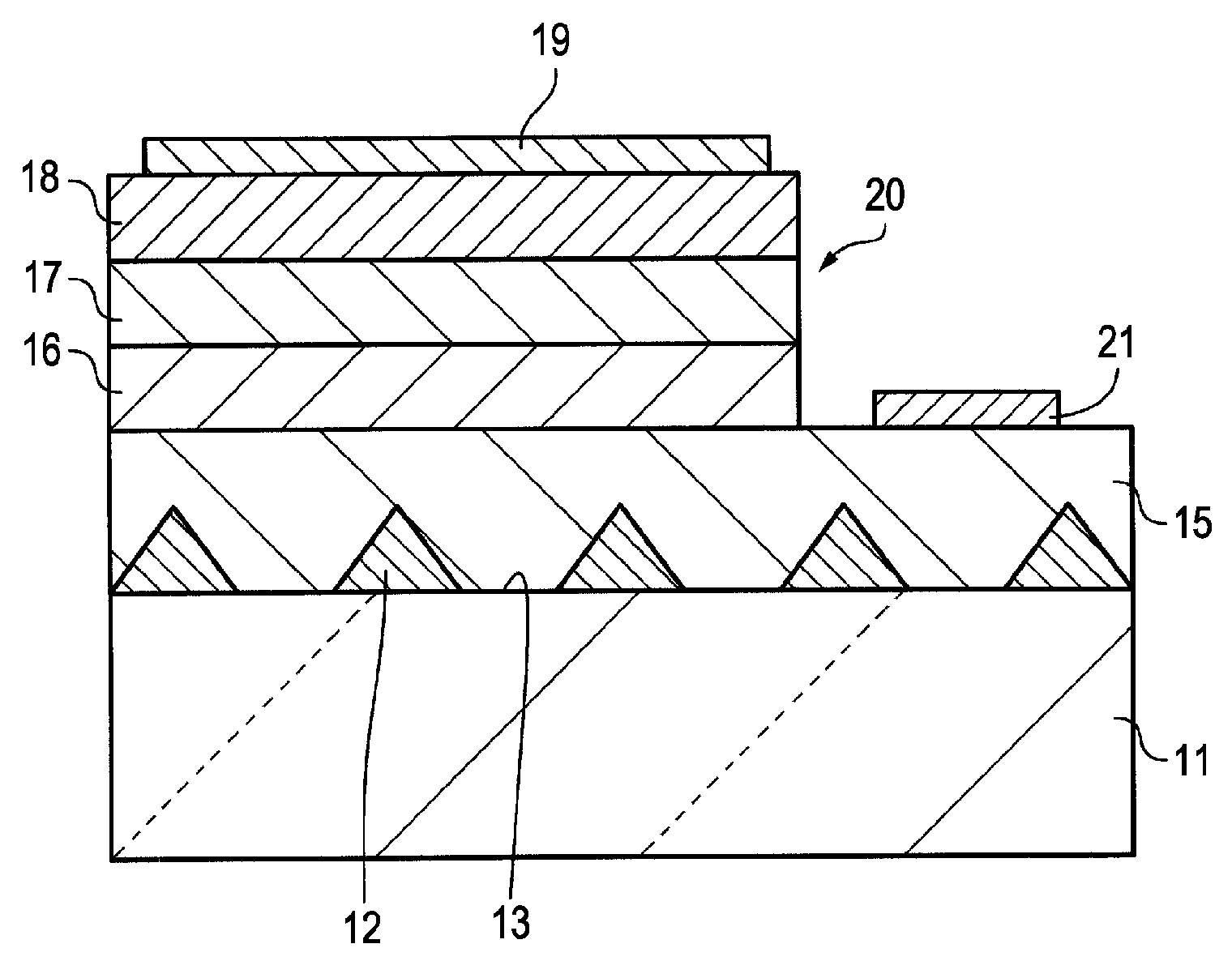
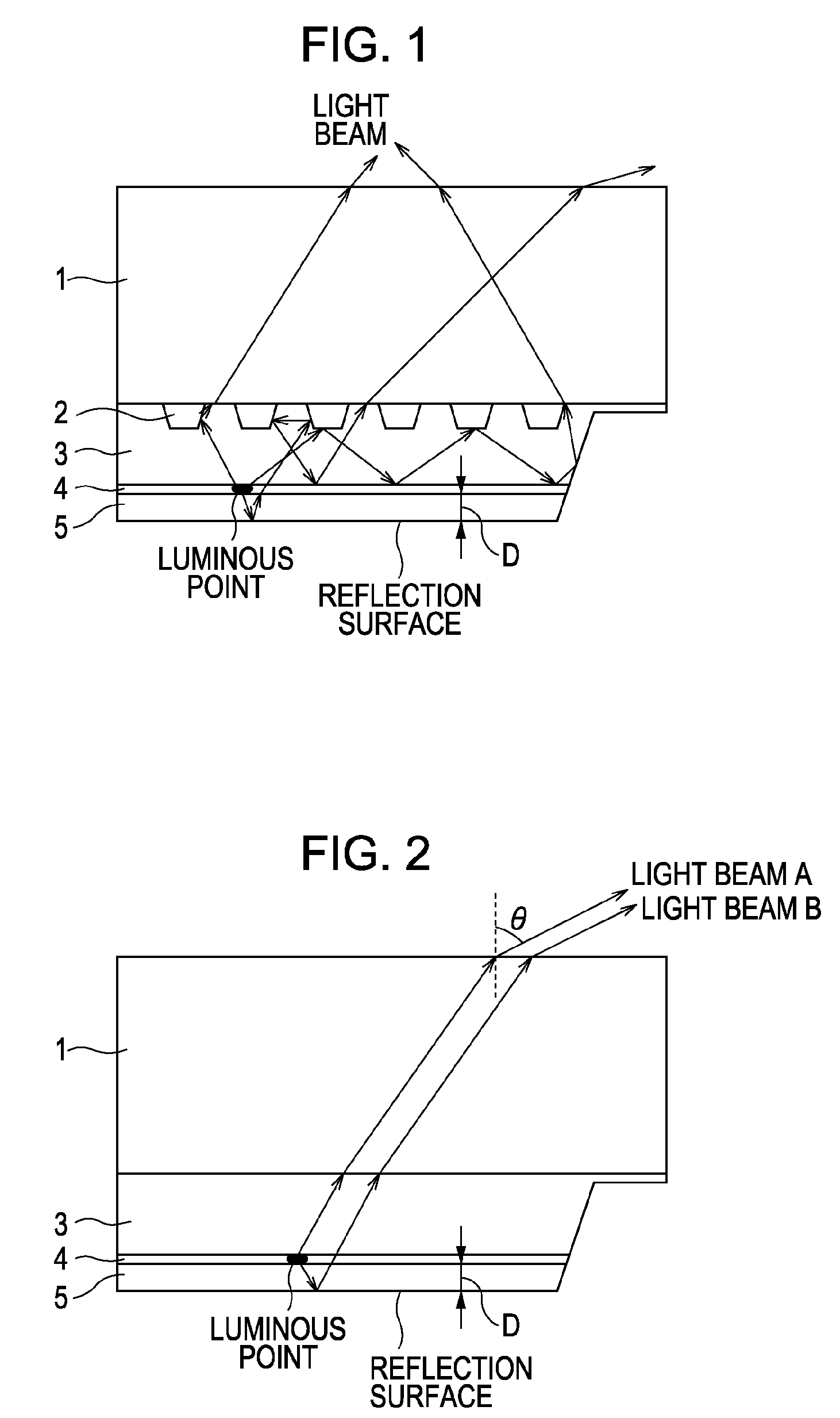
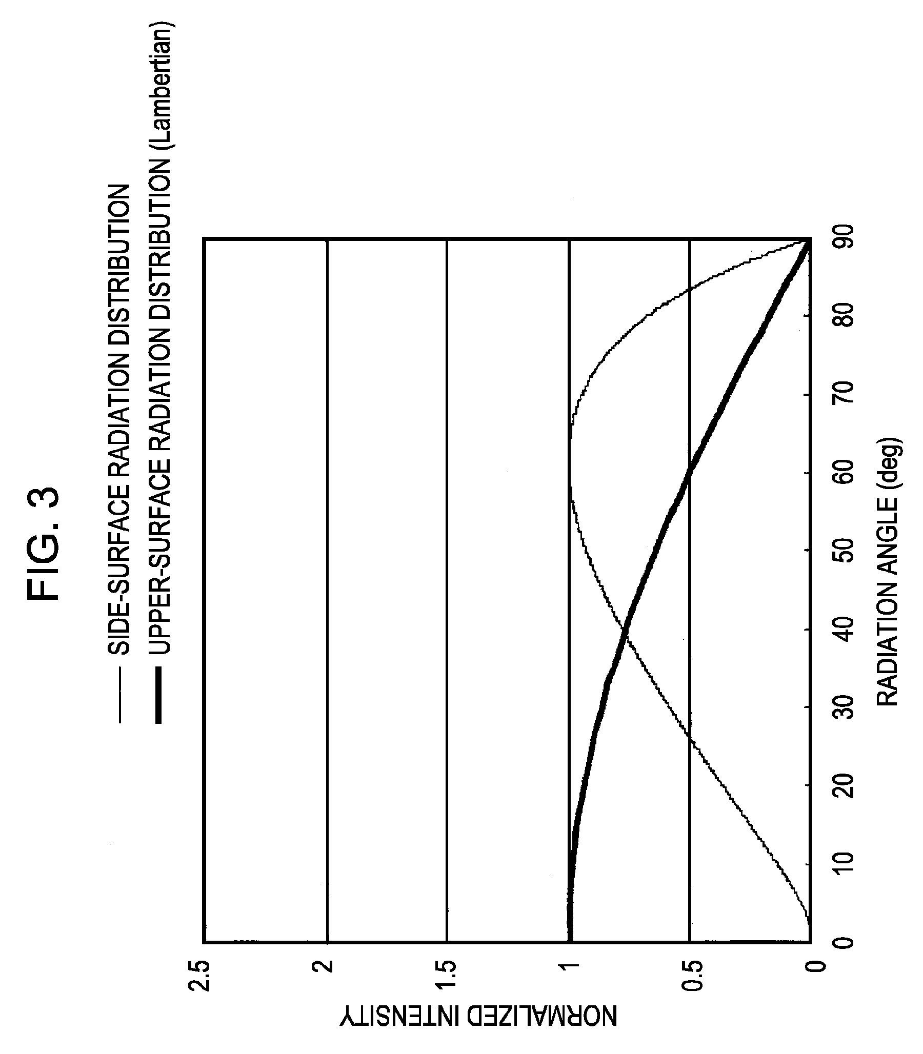
[0177]A light-emitting diode was formed by using Si3N4 having a refractive index of 2.0 as a dielectric substance forming the convex portions 12. As a comparative example, a light-emitting diode was formed by using SiO2 having a refractive index of 1.46 as a dielectric substance forming the convex portions 12. The shape and the arrangement of the convex portions 12 were the same as those shown in FIG. 14. As the p-side electrode 19, a Ag electrode was used. The light-emitting wavelength X of the light-emitting diodes was 530 nm, and the distance D between the center (luminous point) of the active layer 17 having a multiquantum well structure and the reflection surface (interface between the p-type nitride-based III-V compound semiconductor layer 18 and the p-side electrode 19) was approximately 1.11 λn (n indicates the refractive index of the dielectric substance forming the convex portions 12). FIG. 32 shows far-field patterns of the two type of light-emitting diodes, which are nor...


PUM


Abstract

A light-emitting diode which has a significantly high luminous efficiency and which can be manufactured at a reasonable cost by one epitaxial growth and a manufacturing method thereof are provided. The above method includes: preparing a substrate provided with convex portions on one major surface, the convex portions being formed from a dielectric substance which is different from the substrate and which has a refractive index of 1.7 to 2.2; growing a first nitride-based III-V compound semiconductor layer in a concave portion on the substrate; growing a second nitride-based III-V compound semiconductor layer on the substrate from the first nitride-based III-V compound semiconductor layer in a lateral direction; and growing, on the second nitride-based III-V compound semiconductor layer, a first conductive type third nitride-based III-V compound semiconductor layer, an active layer, and a second conductive type fourth nitride-based III-V compound semiconductor layer.

Description

CROSS REFERENCES TO RELATED APPLICATIONS[0001]The present invention contains subject matter related to Japanese Patent Application JP 2006-316885 filed in the Japanese Patent Office on Nov. 24, 2006, the entire contents of which are incorporated herein by reference.BACKGROUND OF THE INVENTION[0002]1. Field of the Invention[0003]The present invention relates to a method for manufacturing a light-emitting diode, a light-emitting diode, a light source cell unit, a light-emitting diode backlight, a light-emitting diode illuminating device, a light-emitting diode display, and an electronic apparatus, and more particularly, relates to a light-emitting diode using a nitride-based III-V compound semiconductor and to various devices and / or apparatuses using this light-emitting diode.[0004]2. Description of the Related Art[0005]When a GaN-based semiconductor is epitaxial-grown on a different type substrate such as a sapphire substrate, since the differences in lattice constant and coefficient...

Claims


Application Information

Patent Timeline
IPC IPC(8): H01L33/00H01L33/10H01L33/06H01L33/22H01L33/32H01L33/42H01L33/56H01L33/62
CPCH01L21/0237H01L21/02458H01L2224/48465H01L2224/48091H01L33/0079H01L33/007H01L21/0254H01L21/0262H01L21/02642H01L21/02647H01L25/0753H01L2924/00014H01L2924/00H01L33/0093
Inventor HIRAMATSU, YUUJIOKANO, NOBUKATAHINO, TOMONORI
Owner SONY CORP
Why Eureka
Try Eureka