Method for Fabrication of Semiconductor Light-Emitting Device and the Device Fabricated by the Method

a technology of light-emitting devices and manufacturing methods, which is applied in the manufacture of tools, laser beam welding apparatuses, welding/soldering/cutting articles, etc., can solve the problems of bringing the luminance of emission of led chips to a lower level, consuming a long time, and requiring only difficulty in materializing the processing done by the conventional method

Active Publication Date: 2008-05-29
TOYODA GOSEI CO LTD
View PDF3 Cites 114 Cited by
  • Summary
  • Abstract
  • Description
  • Claims
  • Application Information

AI Technical Summary

Problems solved by technology

Since a nitride-based compound semiconductor and a substrate for which an SiC and a sapphire is usually used are hard substances comparable to diamond, the processing performed thereon by the use of a dicing saw and a scriber has necessitated a highly advanced technique and consumed a long time.
Since the use of the laser beam is capable of forming trenches narrower and deeper than those of the conventional processing devices, it can materialize the processing which has been accomplished by the conventional method only with difficulty.
The use of the laser-processing device, however, results in bringing the luminance of emission of the LED chip to a lower leve

Method used


Image

  • Method for Fabrication of Semiconductor Light-Emitting Device and the Device Fabricated by the Method
  • Method for Fabrication of Semiconductor Light-Emitting Device and the Device Fabricated by the Method
  • Method for Fabrication of Semiconductor Light-Emitting Device and the Device Fabricated by the Method

Examples


example 1

[0041]A blue light-emitting device formed of a nitride-based compound semiconductor was fabricated as follows.

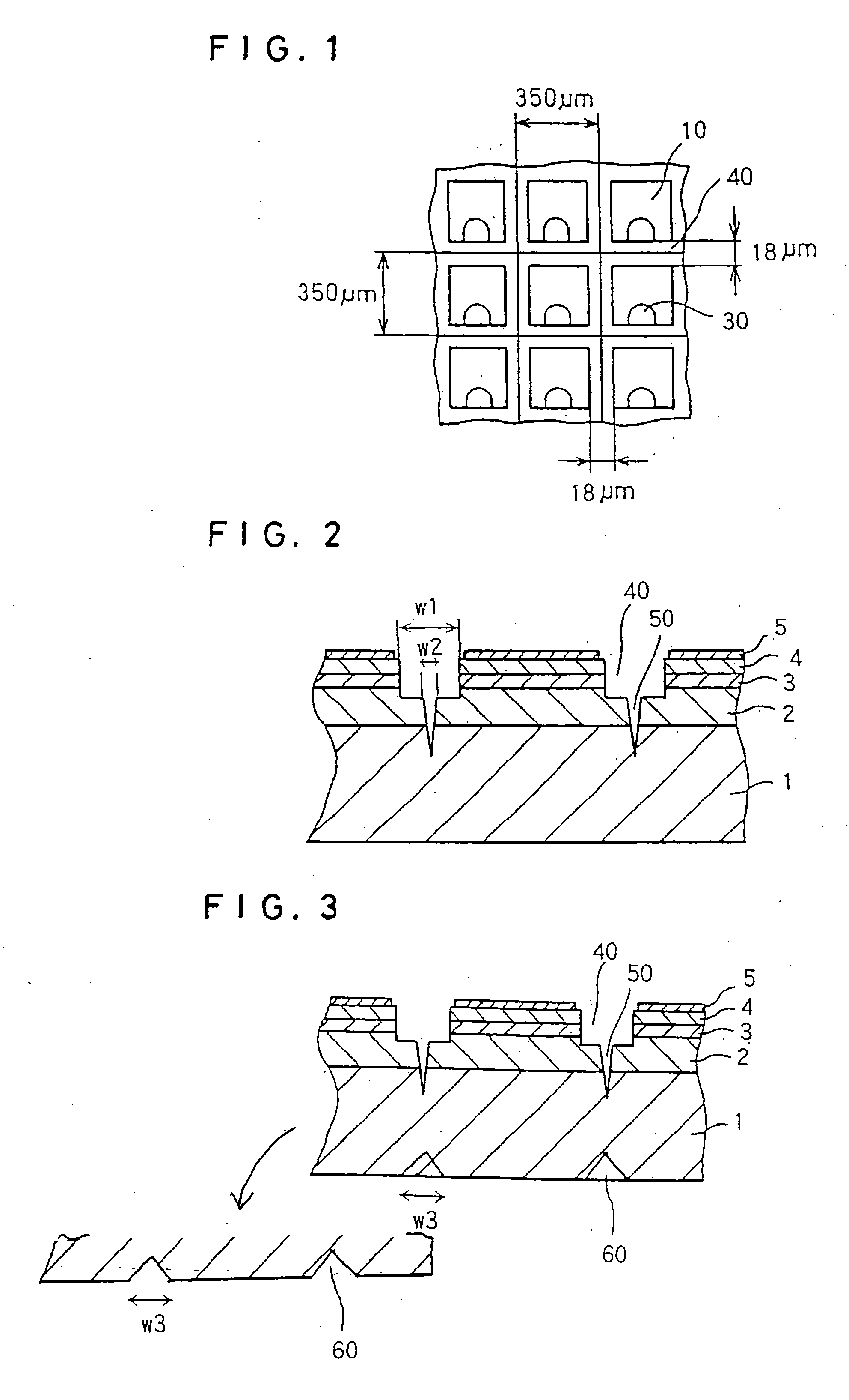
[0042]On a sapphire substrate, an AlN layer, an under layer having a thickness of 4 μm and formed of undoped GaN, an n-side contact layer having a thickness of 2 μm and formed of Ge-doped (concentration 1×10¹⁹ / cm3) GaN, an n-side cladding layer having a thickness of 12.5 nm and formed of Si-doped (concentration 1×10¹⁸ / cm3) Ino.1Gao.9N, a barrier layer having a thickness of 16 nm and formed of GaN and a well layer having a thickness of 2.5 nm and formed of Ino.2Gao.8N are stacked alternatively up to five repetitions, and finally a light-emitting layer of a multiple quantum well structure provided with a barrier layer, a p-side cladding layer having a thickness of 2.5 nm and formed of Mg-doped (concentration 1×10²⁰ / cm3) Alo.o7Gao.93N and a p-side contact layer having a thickness of 0.16 μm and formed of Mg-doped (concentration 8×10¹⁹ / cm3) Alo.02Gao.98N are sequentially stacked...

example 2

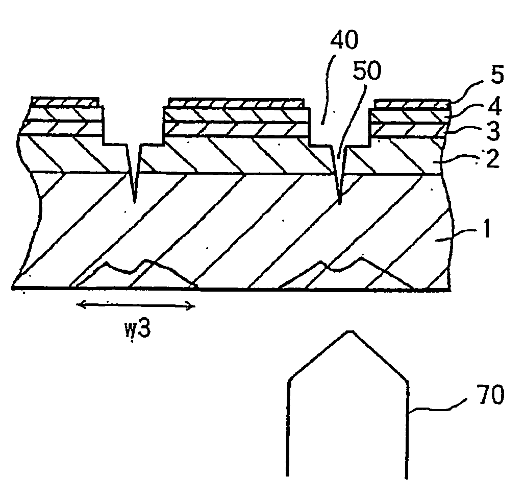
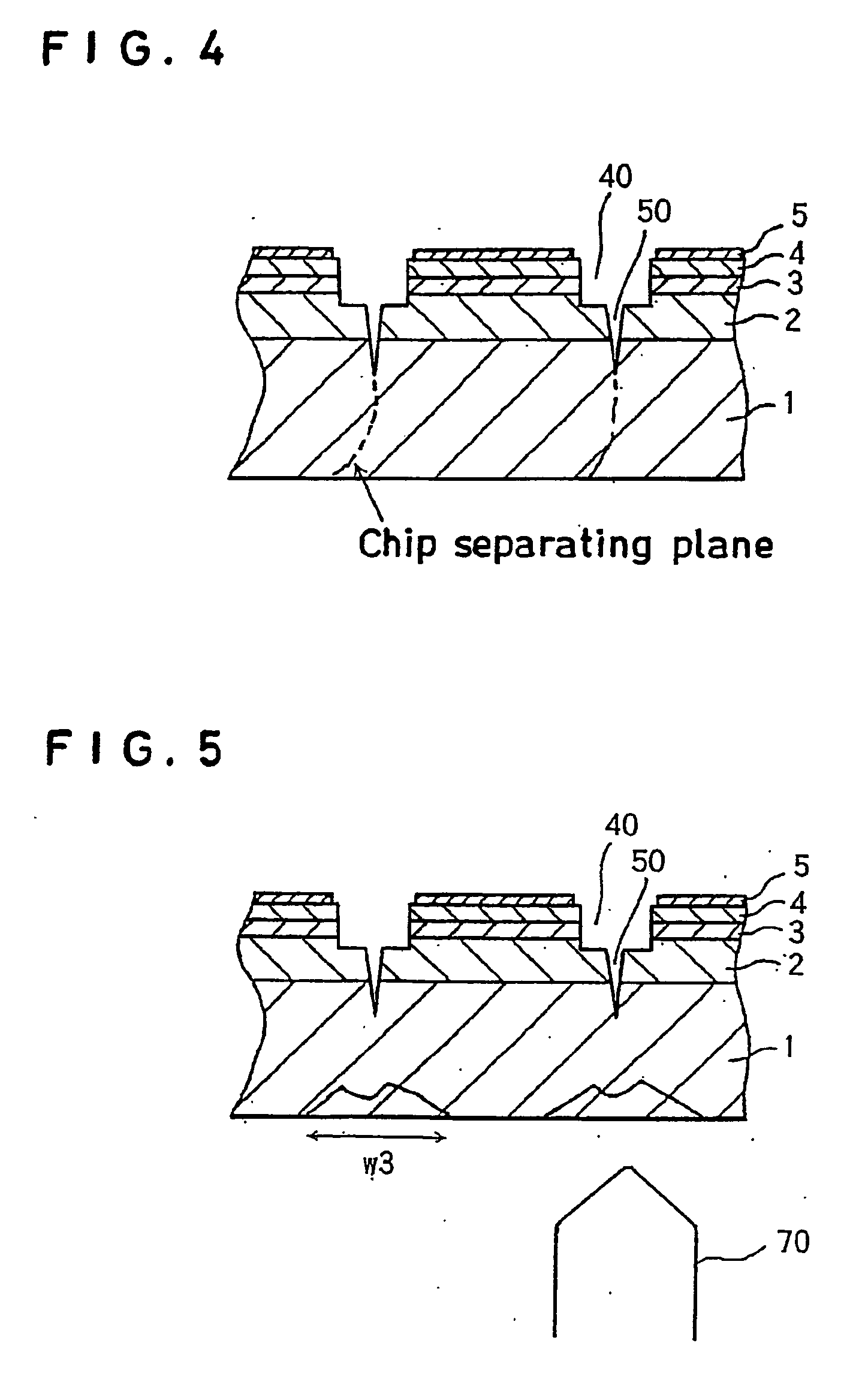
[0051]Nitride-based compound semiconductor light-emitting devices shaped like chips were fabricated by following the procedure of Example 1 while performing the dicing treatment subsequently to the laser processing for the purpose of forming third trenches having a width of 20 μm and a depth of 30 μm. During the formation of the third trenches, the laser beam was radiated so as to form the focal point at a position separated by about 30 μm from the substrate. After the irradiation with the laser beam was completed, the third trenches were shaped with a width of 20 μm and a depth of 15 μm. Subsequently, the third trenches were corrected in shape by the laser processing treatment using a diamond blade having a V-shaped edge as illustrated in FIG. 5 and a blade width of 20 μm. After the correction of the shape was completed, the third trenches were found to have a width of 20 μm and a depth of 30 μm. This wafer was divided to afford chips. The end faces of these chips were substantiall...

example 3

[0053]Nitride-based compound semiconductor light-emitting devices shaped like chips were fabricated by following the procedure of Example 1 while performing the laser processing treatment in two stages so as to form the third trenches having a width of 20 μm and a depth of 30 μm. In the laser processing of the first stage, the laser was radiated so as to form the focal point thereof at a position separated by about 30 μm from the substrate. The third trenches after the radiation of the laser beam had a width of 20 μm and a depth of 15 μm and assumed a W-latter cross section which resulted from the upward swell of the approximately central portions of the bottom parts thereof. The radiation of the laser beam in the second stage was performed with the focal point directed toward the approximate center of the W-letter cross section. The completed third trenches measured 20 μm in width and 35 μm in depth and assumed a nearly V-shaped groove, though slightly distorted as compared with th...


PUM

PropertyMeasurementUnit
Thicknessaaaaaaaaaa
Electrical conductoraaaaaaaaaa
Widthaaaaaaaaaa

Abstract

A method for producing a semiconductor light-emitting device includes stacking at least a first conductive type semiconductor layer (2), an active layer (3) and a second conductive type semiconductor layer (4) on a substrate (1) to form a wafer, then forming on a side of growth surfaces of the semiconductor layers first trenches (40) exposing the first conductive type semiconductor layer, further forming second trenches (50) reaching the substrate from above the first trenches by using a laser beam, subsequently forming third trenches (60) from the substrate at the positions corresponding to the second trenches, and finally cutting the wafer into chips. The produced semiconductor chips provide an enhanced efficiency of extracting emitted light even when the end faces thereof are smooth surfaces and they allow the semiconductor layer to be cut without distorting the end faces of the chips.

Description

CROSS REFERENCE TO RELATED APPLICATIONS[0001]This application is an application filed under 35 U.S.C. § 111(a) claiming the benefit pursuant to 35 U.S.C. §119(e)(1) of the filing dates of Provisional Application No. 60 / 605,500 filed Aug. 31, 2004 and Japanese Patent Application No. 2004-240764 filed Aug. 20, 2004 pursuant to 35 U.S.C. § 111(b).TECHNICAL FIELD[0002]This invention relates to a method for the fabrication of a semiconductor light-emitting device. More particularly, this invention relates to a light-emitting device of high luminance so severed as to acquire a clean and smooth surface and provide an improved efficiency of light extraction from a light-emitting chip and to a method for the fabrication thereof.BACKGROUND ART[0003]The process for fabricating a light-emitting device by severing into chips a nitride-based compound semiconductor wafer resulting from stacking an n-type layer, an active layer and a p-type layer on an insulating substrate, such as a sapphire subst...

Claims


Application Information

Patent Timeline
IPC IPC(8): H01L21/78H01L33/00H01L33/06H01L33/32H01L33/40
CPCB23K26/4075H01L33/20H01L33/0095H01L21/78B23K26/40B23K2103/50
Inventor YAKUSHIJI, KENJI
Owner TOYODA GOSEI CO LTD
Why Eureka
Try Eureka