Semiconductor devices with MIM-type decoupling capacitors and fabrication method thereof

a technology of decoupling capacitor and semiconductor device, which is applied in the direction of semiconductor device, capacitor, electrical apparatus, etc., can solve the problems of large voltage fluctuations in supply lines, internal signal noise, and voltage noise thereon

Inactive Publication Date: 2008-05-29
TAIWAN SEMICON MFG CO LTD
View PDF5 Cites 31 Cited by
  • Summary
  • Abstract
  • Description
  • Claims
  • Application Information

AI Technical Summary

Problems solved by technology

During operation of circuits, the power supply lines supply transient current with a relatively high intensity, resulting in voltage noise thereon.
In such circuits, the rising time of clock signals is very short, resulting in large voltage fluctuations in the supply lines.
Undesired voltage fluctuations in power supply lines powering a circuit cause noise in internal signals and degrade noise margins.
The degradation of noise margins reduces circuit reliability and can even cause circuit malfunction.
MOS type capacitors suffer from capacitance variations caused by the doping characteristics of the polysilicon capacitor electrode plates, and as such, these devices exhibit fairly large changes in the capacitance as a function of applied voltage.
Hence, these devices have a large voltage coefficient of capacitance.
In addition, the parasitic effect occurs in MOS type transistors where the capacitor is located near the substrate.
Moreover, integration of the high-k dielectric layer sandwiched between the metal electrodes is difficult due to the high-temperature processes of the BEOL.

Method used


Image

  • Semiconductor devices with MIM-type decoupling capacitors and fabrication method thereof
  • Semiconductor devices with MIM-type decoupling capacitors and fabrication method thereof
  • Semiconductor devices with MIM-type decoupling capacitors and fabrication method thereof

Examples


Embodiment Construction

[0022]The following description is of the best-contemplated mode of carrying out the invention. This description is made for the purpose of illustrating the general principles of the invention and should not be taken in a limiting sense. The scope of the invention is best determined by reference to the appended claims.

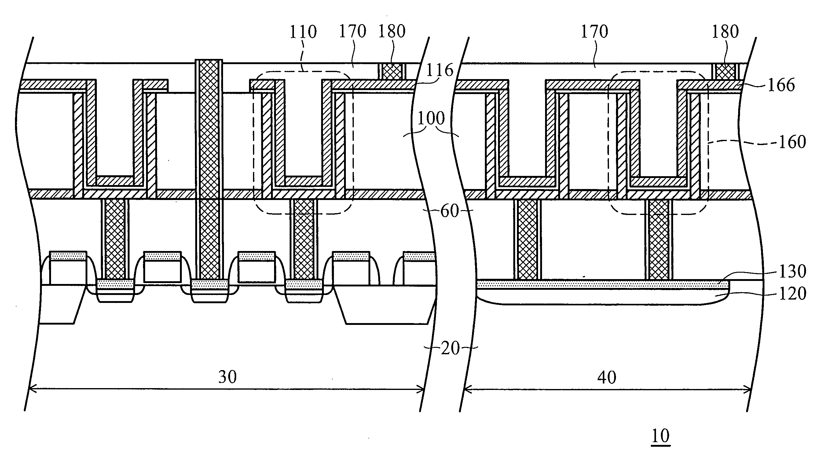
[0023]The invention provides a semiconductor device comprising a substrate having an array region and a decoupling region, a first dielectric layer overlying the substrate, a second dielectric layer overlying the first dielectric layer, a plurality of active components formed in the first dielectric layer within the array region, a first capacitor formed in the second dielectric layer within the array region, a second capacitor formed in the second dielectric layer within the decoupling region, and a first plug formed in the first dielectric layer within the array region electrically connecting the active component and the first capacitor.

[0024]The substrate may compri...


PUM


Abstract

A semiconductor device. The semiconductor device includes a substrate having an array region and a decoupling region, a first dielectric layer overlying the substrate, a second dielectric layer overlying the first dielectric layer, a plurality of active components formed in the first dielectric layer within the array region, a first capacitor formed in the second dielectric layer within the array region, a second capacitor formed in the second dielectric layer within the decoupling region, and a first plug formed in the first dielectric layer within the array region electrically connecting the active component and the first capacitor. The invention also provides a method of fabricating the semiconductor device.

Description

BACKGROUND OF THE INVENTION[0001]1. Field of the Invention[0002]The invention relates to a semiconductor device, and in particular to a semiconductor device with a metal-insulator-metal (MIM) type decoupling capacitor and a fabrication method thereof.[0003]2. Description of the Related Art[0004]Power supply lines in a semiconductor integrated circuit chip supply current to charge and discharge active and passive devices in the integrated circuit. For example, digital complementary metal-oxide-semiconductor (CMOS) circuits draw current when the clock makes a transition. During operation of circuits, the power supply lines supply transient current with a relatively high intensity, resulting in voltage noise thereon. The voltage on the power supply lines fluctuates when the fluctuation time of the transient current is short or when its parasitic inductance or parasitic resistance is large. In state-of-the-art circuits, the operational frequency of the integrated circuit is on the order...

Claims


Application Information

Patent Timeline
Patent Type & Authority Applications(United States)
IPC IPC(8): H01L29/00H01L21/02
CPCH01L28/91H01L28/55
Inventor TU, KUO-CHICHEN, CHUN-YAO
Owner TAIWAN SEMICON MFG CO LTD
Why Eureka
Try Eureka