Manufacturing Method Of Semiconductor Device And Semiconductor Device Produced Therewith

a manufacturing method and semiconductor technology, applied in semiconductor devices, semiconductor/solid-state device details, electrical devices, etc., can solve the problems of deterioration of the wiring layer, rise in the dielectric constant or mechanical strength, peeling, etc., to achieve less leakage current, increase parasite capacitance can be sufficiently suppressed, and high adhesion

Active Publication Date: 2008-05-29
ROHM CO LTD +1
View PDF16 Cites 21 Cited by
  • Summary
  • Abstract
  • Description
  • Claims
  • Application Information

AI Technical Summary

Benefits of technology

[0075]According to the method of the invention, before a plasma treatment is applied as a pretreatment for forming a conductive layer by means of the sputtering method, a gas containing at least one kind of TMCTS, HMDS and TMCS molecules is brought into contact with a surface to impart the plasma resistance...

Problems solved by technology

Accordingly, even when a dielectric thin film high in the pore rate and low in the dielectric constant can be formed, because of high pore rate, in subsequent various processes including a patterning process, in many cases, etching residue sticks to the inside of the pores, resulting in causing a rise in the dielectric constant or a deterioration in the mechanical strength.
However, there are problems in that, in actuality, the as-designed dielectric constant cannot be obtained to result in, in some cases, causing the leakage current, and, furthermore, owing to poor adhesion with the wiring layer, the peeling tends to occur.
In particular, there are problems in that, when a dielectric thin film having a hydrophobicized surface is exposed to a reac...

Method used


Image

  • Manufacturing Method Of Semiconductor Device And Semiconductor Device Produced Therewith
  • Manufacturing Method Of Semiconductor Device And Semiconductor Device Produced Therewith
  • Manufacturing Method Of Semiconductor Device And Semiconductor Device Produced Therewith

Examples


embodiment 1

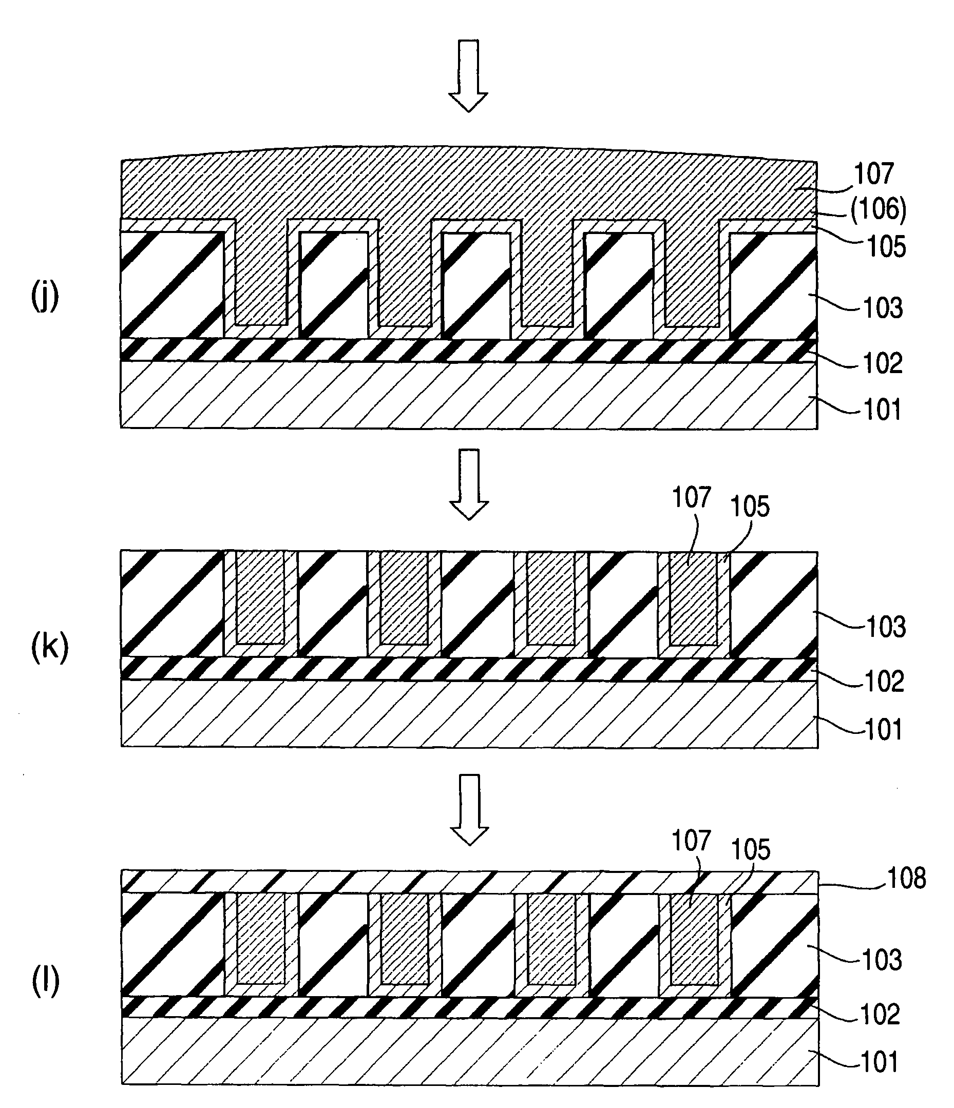
[0120]As an embodiment 1 of the invention, a manufacturing method of a single damascene wiring structure in which the dielectric thin film is used as an interlayer insulating film of a semiconductor device will be described.

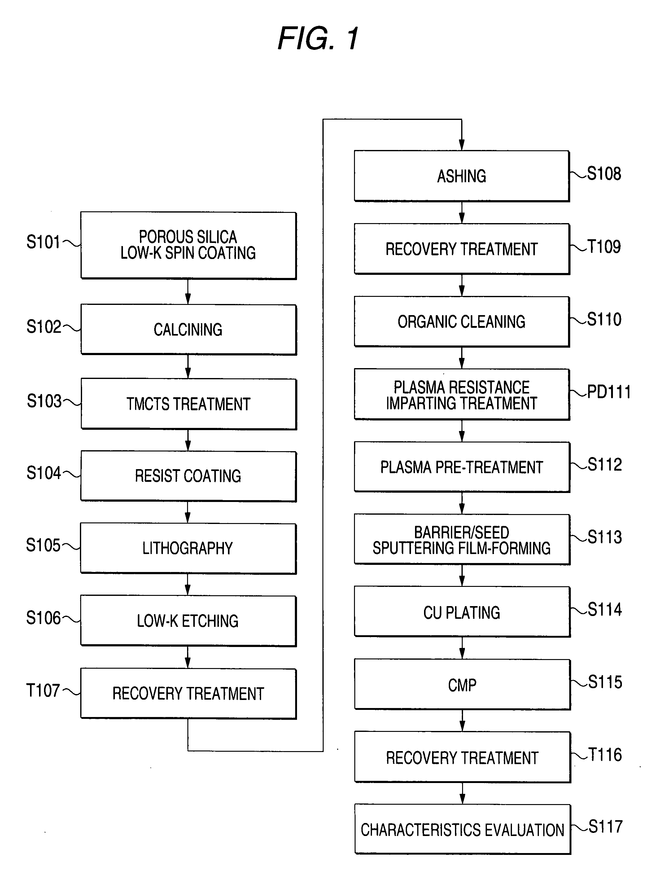
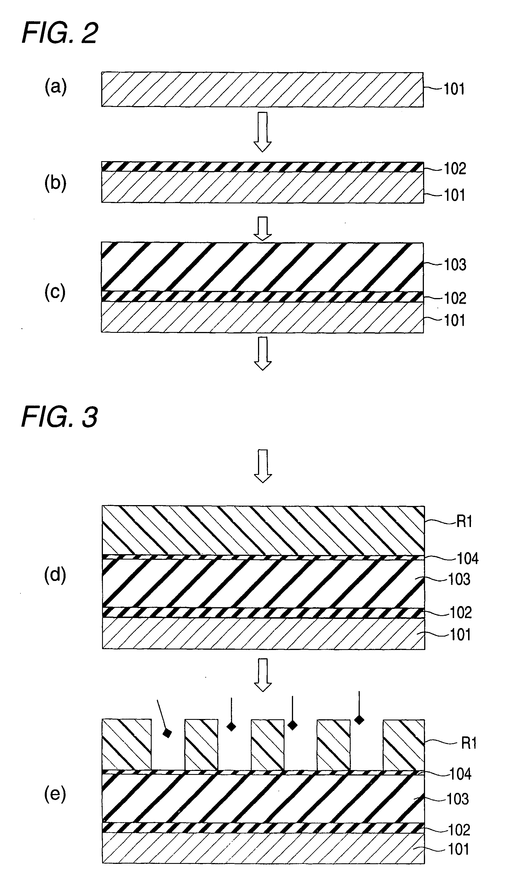
[0121]In the method, as shown in a flowchart in FIG. 1 and production process diagrams shown in FIGS. 2(a) through 6(l), when an interlayer insulating film having a single damascene wiring structure is formed from a dielectric thin film made of a mesoporous silica thin film and on the dielectric thin film a wiring layer is formed by means of the sputtering method, before a plasma pretreatment with argon / helium / nitrogen / hydrogen plasma, a step of bringing into contact with TMCTS molecules to impart the plasma resistance is included.

[0122]As the process, before a step of forming a wiring layer in the existing process, a step of bringing into contact with TMCTS molecules (resistance imparting step) and a step of argon / helium / nitrogen / hydrogen plasma treatment are in...

embodiment 2

[0184]In the embodiment 1, a production process of a semiconductor device, which contains a step where a groove is formed in an interlayer insulating film with a resist pattern as a mask was described. In the present embodiment, formation of a groove by use of a hard mask having a two-layered structure will be described. In the embodiment as well, similarly, a manufacturing method of a single damascene wiring structure will be described.

[0185]The method is similar to that described in the embodiment 1 only except that, as production process charts are shown in FIGS. 17(a) through 21(n), as a hard mask, a two-layer structure mask made of a silicon oxide film 201 and a silicon nitride film 202 is used. In the method, a plasma resistance imparting treatment step of forming an interlayer insulating film having the single damascene wiring structure from a dielectric thin film made of a mesoporous silica thin film, and, before the sputtering, bringing into contact with TMCTS molecules; an...

embodiment 3

[0201]In the embodiment 2, a manufacturing step of a semiconductor device, which contains a step where a groove is formed in an interlayer insulating film with a two-layer structure hard mask as a mask was described. In the present embodiment, formation of a groove with a single-layer hard mask will be described. In the embodiment as well, similarly, a manufacturing method of a single damascene wiring structure will be described.

[0202]The method is similar to that described in the embodiment 2 only except that, as production process charts are shown in FIGS. 22(a) through 26(n), as a hard mask, a silicon carbide film 301 is used. In the method, an interlayer insulating film having the single damascene wiring structure is formed of a dielectric thin film made of a mesoporous silica thin film, before the sputtering, a plasma resistance imparting treatment step of bringing into contact with TMCTS molecules and a recovery treatment step of applying pretreatment with plasma to form a wir...


PUM


Abstract

A semiconductor device having a wiring structure that is enhanced in adhesion between a dielectric thin film and a conductive layer and has high reliability is provided.
A method of the invention includes: a step of supplying reactive plasma on a surface of a dielectric thin film in which a plurality of pores are arranged around a skeleton mainly made of a Si—O bond, to perform a pretreatment; a step of forming a conductive film on the surface of the pretreated dielectric thin film by a sputtering method; and before the pretreatment step, bringing a gas containing at least one kind of tetramethylcyclotetrasiloxane (TMCTS), hexamethylsilazane (HMDS) and trimethylchlorosilane (TMCS) molecules into contact with the surface of the dielectric thin film.

Description

TECHNICAL FIELD[0001]The invention relates to a manufacturing method of a semiconductor device and a semiconductor device produced therewith, in particular, to a surface treatment technology of a dielectric thin film for avoiding damage due to plasma in a plasma treatment step.RELATED ART[0002]In order to realize high speed / low power consumption of a semiconductor device, it is very important to lower the dielectric constant of an interlayer insulating film. In order to lower the dielectric constant, there have been proposed various devises. The inventors proposed a dielectric thin film in which pores are regularly arranged (patent literature 1).[0003]Furthermore, as a modification method of a porous film, a method where an organic silicon compound is brought into contact with the porous film made of a Si—O bond to thermally treat without using a metal catalyst to improve the hydrophobicity and the mechanical strength is proposed as well (patent literature 2).[0004]Although a dielec...

Claims


Application Information

Patent Timeline
IPC IPC(8): H01L23/48H01L21/4763
CPCH01L21/2855H01L21/32051H01L21/76802H01L21/76843H01L21/76826H01L21/76832H01L21/76834H01L21/7682H01L2221/1047H01L21/768
Inventor OKU, YOSHIAKIFUJII, NOBUTOSHIKOHMURA, KAZUO
Owner ROHM CO LTD
Why Eureka
Try Eureka