Electrochemical device and methods for producing the same

a technology of electrochemical transistors and electrochemical devices, which is applied in thermoelectric devices, instruments, nanoinformatics, etc., can solve the problems of affecting the practical use of prior art electrochemical transistor devices, affecting the practical use of electrochemical transistor devices, and requiring high manufacturing costs

Inactive Publication Date: 2008-06-05
ACREO
View PDF14 Cites 14 Cited by
  • Summary
  • Abstract
  • Description
  • Claims
  • Application Information

AI Technical Summary

Benefits of technology

[0007]Yet another object of the present invention is to provide an environmentally safe electrochemical transistor device, so that the disposal of the device, along with any support onto which it has been deposited, doesn't give rise to handling problems, and so that no safety restrictions have to be imposed on the use of the device.
[0048]Many basic circuits, such as inverters, AND, NAND, OR, and NOR operators, may be formed out of interconnected transistors and resistors. Hence, the present invention provides the hitherto missing part (i.e. the transistor) for making cheap, printable, and environmentally friendly circuitries that can be arranged on e.g. a flexible substrate such as a piece of paper.

Problems solved by technology

Problems with electrochemical transistor devices of the prior art include the fact that they are difficult and expensive to manufacture.
In particular, no electrochemical transistor devices have been disclosed which are capable of being mass-produced.
Furthermore, the practical use of prior art electrochemical transistor devices has been hampered by their comparatively high power consumption.
Furthermore, materials used in prior art devices suffer from a lack of environmental friendliness, processability and economic production possibilities.

Method used


Image

  • Electrochemical device and methods for producing the same
  • Electrochemical device and methods for producing the same
  • Electrochemical device and methods for producing the same

Examples


experiment 1

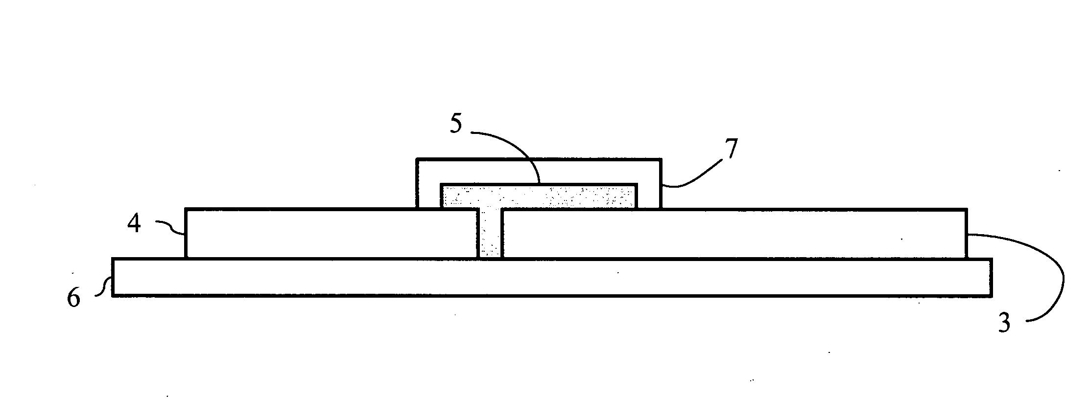
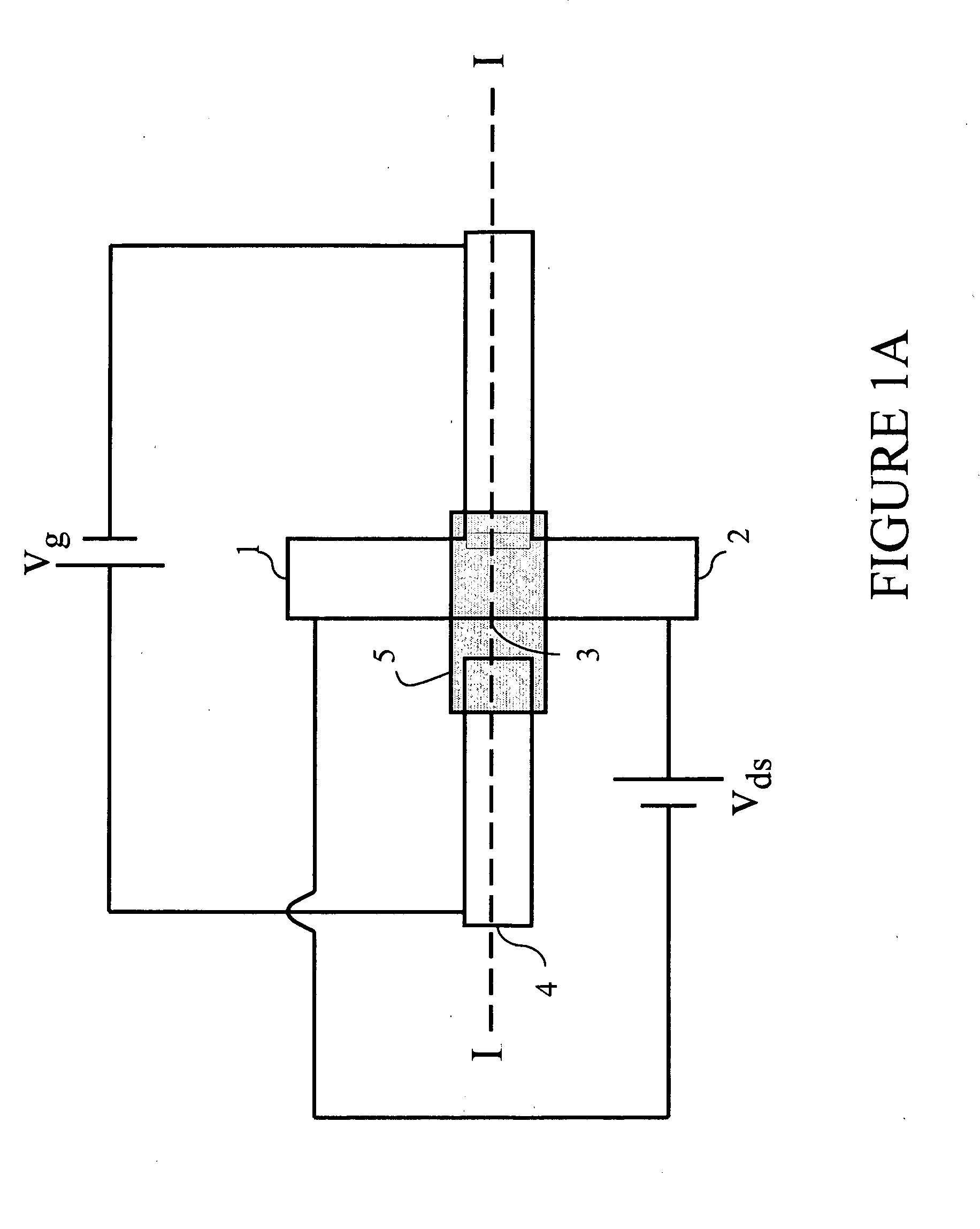
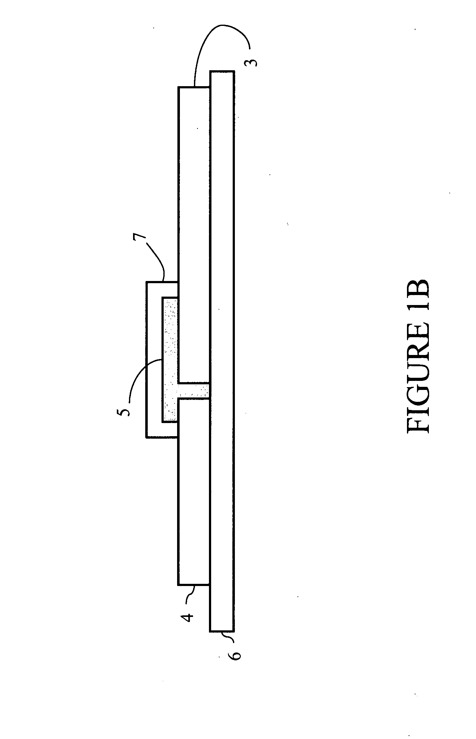
[0129]Bi-stable transistor: A bi-stable transistor such as that shown schematically in FIGS. 1A and 1B was realized. The bi-stable transistor had a transistor channel width of 600 μm and a gel width of 800 μm, with a transistor channel of 0.48 cm2. However, smaller dimensions were also successfully tested using photolithographic photoresist patterning in combination with reactive ion plasma etching. These devices exhibited channel widths ranging from 5 to 20 μm and a gel width of 20 μm.

[0130]Typically, the gate voltages Vg applied to the gate electrode were in the interval between 0 V and 0.7 V. Drain-source characteristics were determined by sweeping the source-drain voltage from 0 V to 2 V. The resulting I-V curves are displayed in FIG. 4.

[0131]Characteristic switching times for the conductivity modulation were determined by applying a square shaped modulation voltage (alternating between 0 V and 1 V) and measuring the resulting current changes. Typical rise and decline times (def...

experiment 2

[0139]Bi-stable transistors such as that shown schematically in FIGS. 1A and 1B were realized. The bi-stable transistors had a transistor channel width of 3 mm and a gel width of 4 mm, with a transistor channel of 12 mm2. Typically, the gate voltages Vg applied to the gate electrode were in the interval between −15 V and 15 V. Drain-source characteristics were determined by sweeping the source-drain voltage from 0 V to 10 V. The resulting I-V curves are displayed in FIG. 6 (polyaniline supplied in toluene solution) and FIG. 7 (polyaniline supplied in m-cresol solution).

[0140]On / Off ratios (defined as the current ratio Ids,max / lds,min at a source-drain voltage Vds of 2 V for Vg=0 V (on) and Vg=4 V or −4 V (off)) reached 100 for both negative and positive gate voltages.

Three-Terminal Transistors

[0141]Due to the impracticality to design circuits based on transistors with floating gate supplies a three-terminal transistor having a fixed gate supply will be described in the following. In...


PUM

PropertyMeasurementUnit
gate voltage Vgaaaaaaaaaa
line widthsaaaaaaaaaa
distanceaaaaaaaaaa

Abstract

Methods of producing electrochemical transistor devices are provided, wherein a solidified electrolyte is arranged in direct contact with at least a portion of an organic material having the ability to electrochemically altering its electrical conductivity through change of redox state thereof, such that a current between a source contact and a drain contact of the transistor is controllable by way of a voltage applied to a gate electrode. A electrochemical transistor device is also provided, wherein an ion isolative material is provided between a solidified electrolyte and an organic material having ability to electrochemically altering its redox state, such that a transistor channel of the transistor is defined thereby.

Description

[0001]This is a divisional application of parent U.S. patent application Ser. No. 11 / 327,438, filed Jan. 9, 2006, which is a continuation of U.S. patent application Ser. No. 10 / 819,306, filed Apr. 7, 2004 (now U.S. Pat. No. 7,012,306), which in turn is a Continuation-in-Part of U.S. patent application Ser. No. 10 / 091,419 filed Mar. 7, 2002 (now U.S. Pat. No. 6,806,511), claiming the benefit under 35 U.S.C. §119(a)-(d) of Swedish Application No. 0100748-3, filed Mar. 7, 2001 and under 35 U.S.C. §119(e) of U.S. Provisional Application No. 60 / 276,218, filed Mar. 16, 2001, the entire contents of each of which are hereby incorporated herein by reference.FIELD OF THE INVENTION[0002]The present invention relates to electrochemical devices, in particular to printable, electrochemical transistor devices based on conducting organic materials and methods of producing such devices.BACKGROUND OF THE INVENTION[0003]Semiconducting and conducting organic materials, both polymers and molecules, have...

Claims


Application Information

Patent Timeline
Patent Type & Authority Applications(United States)
IPC IPC(8): H01L51/05H01L51/40C09K9/02G02F1/163G11C13/02H01L21/02H01L21/316H01L51/00H01L51/30
CPCB82Y10/00C09K9/02H01L2924/0002G02F1/163G02F2001/1635G02F2202/022G11C13/0009G11C13/0014G11C13/0016G11C2213/15H01L21/31604H01L27/283H01L28/56H01L51/0037H01L51/0097H01L51/0508H01L51/052H01L2924/00H10K19/10H10K85/1135H10K10/46H10K10/471H10K77/111H01L21/02263
Inventor ARMGARTH, MARTENCHEN, MIAIOXIANG M.NILSSON, DAVID A.BERGGREN, ROLF M.KUGLER, THOMASREMONEN, TOMMI M.FORCHHEIMER, ROBERT
Owner ACREO
Why Eureka
Try Eureka