Light emitting device and method of manufacturing the same
Inactive Publication Date: 2008-06-05
SONY CORP
View PDF14 Cites 42 Cited by
Summary
Abstract
Description
Claims
Application Information
AI Technical Summary
This helps you quickly interpret patents by identifying the three key elements:
Problems solved by technology
Method used
Benefits of technology
Benefits of technology
[0062]In the present invention, the second electrode is covered with an SOG layer. The SOG material layer serving as a kind of precursor (SOG layer precursor) for forming the SOG layer is liquid, and the second electrode can be covered with the SOG material layer by a coating method. Therefore, the second electrode can be assuredly covered with a continuous film free of grain boundaries, and generation of pinholes or cracks can be obviated. As a result, moisture (water) from the external atmosphere can be securely prevented from reaching the second electrode including silver (Ag) or ITO, whereby it is possible to securely obviate the problem that ion migration is generated or whiskers are formed in the second electrode, leading to deterioration of the second electrode and, hence, to deterioration of characteristics of the light emitting diode. Therefore, it is possible to contrive enhanced reliability of the light emitting device, to maintain stable characteristics even under severe environmental conditions, and to achieve an increase in the yield of the light emitting device.
Problems solved by technology
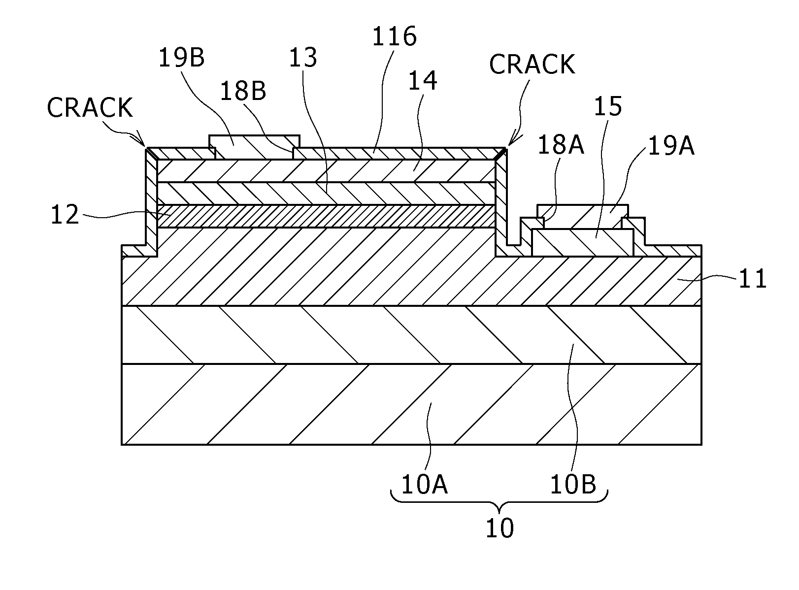
Meanwhile, pinholes and cracks are liable to be generated in the insulating film 116 formed based on a CVD method or a PVD method, and, in the case where a steep stepped part is present extending from the electrode structure or the device structure, it may be impossible to securely cover such a stepped part with the insulating film 116.
In addition, pinholes and cracks may in some cases be generated in the insulating film 116 due to the presence of contamination, foreign matter or the like.
However, these methods are liable to produce other problems due to the influence of heat history, plasma damage or the like.
In addition, it is difficult to securely cover a steep stepped part with the insulating film 116, and such a stepped part will in many cases serve as a discontinuity point in film growth of the insulating film 116.
Method used
Image
Click on the blue label to locate the original text in one second.
Reading with bidirectional positioning of images and text.
Examples
example 1
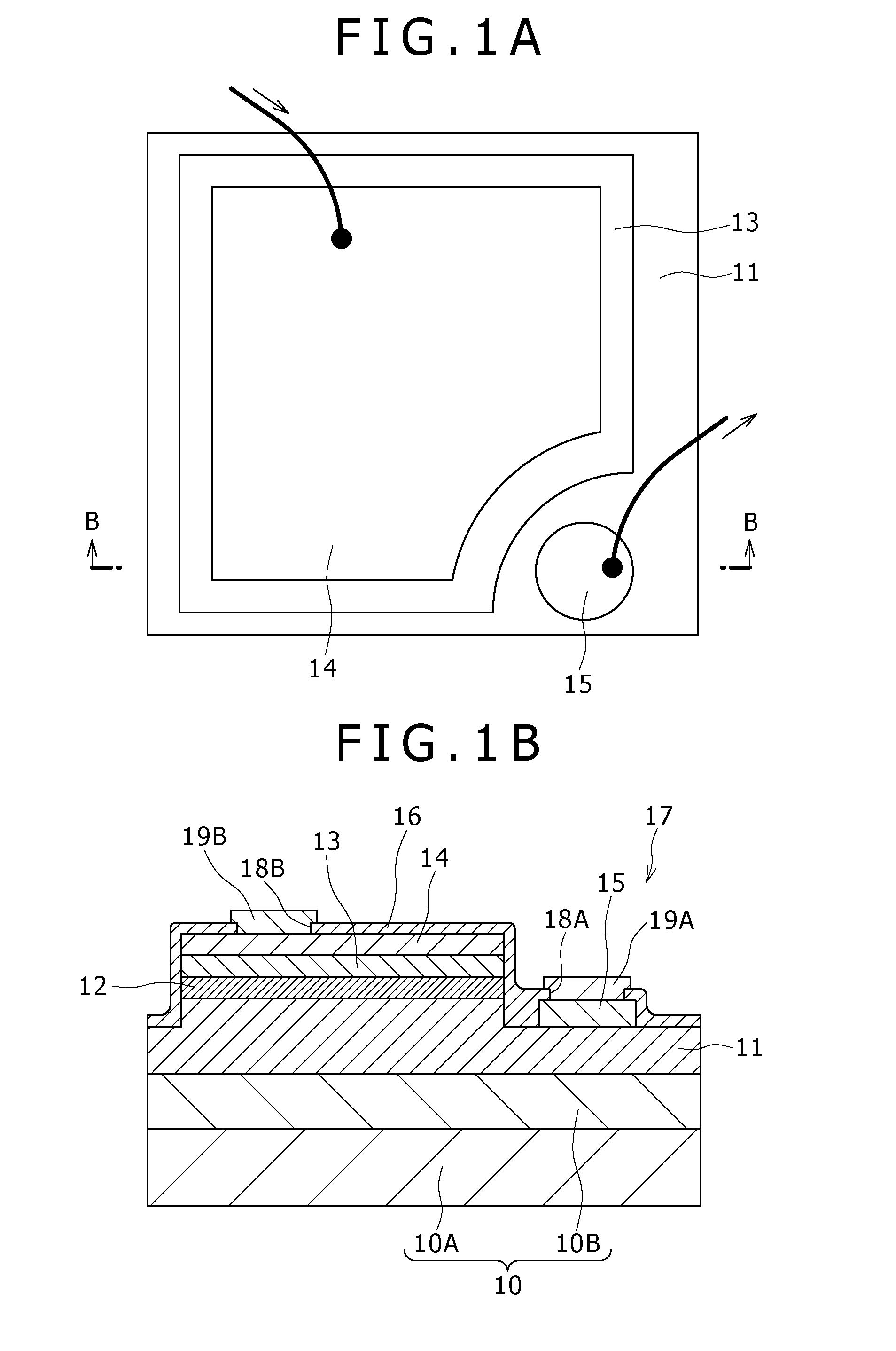
[0074]Example 1 relates to a method of manufacturing a light emitting device according to a first embodiment of the present invention, and the light emitting device based on the present invention.
[0075]The light emitting device according to Example 1 includes a light emitting diode including GaN based compound semiconductor layers, and, as a schematiclayout view of components is shown in FIG. 1A and a schematic sectional view is shown in FIG. 1B taken along line B-B of FIG. 1A, the light emitting device includes:
[0076](a) a first compound semiconductor layer 11 of a first conduction type (n type, in Example 1), an active layer 12, and a second compound semiconductor layer 13 of a second conduction type (p type, in Example 1) different from the first conduction type, which are sequentially formed over a substrate 10;
[0077](b) a first electrode 15 formed over an exposed part 17 of the first compound semiconductor layer 11; and
[0078](c) a second electrode 14 formed over the second com...
example 2
[0097]Example 2 is a modification of Example 1. In Example 2, the second electrode 14 includes a layer of silver (Ag) formed by a vacuum evaporation method and having a thickness of about 100 nm. The light emitting diode in Example 2 is of the substrate-side light pickup type, in which the light emitted from the active layer 12 is transmitted directly through the substrate 10 to go out to the exterior, or is reflected by the second electrode 14 to be transmitted through the substrate 10 and to go out to the exterior. With the second electrode 14 including silver (Ag), a reflectance of not less than 96%, for example, can be attained.
[0098]Incidentally, the other steps and the configurations and structures of the light emitting diode in Example 2 can be made to be the same as in Example 1, and detailed description of them is therefore omitted.
example 3
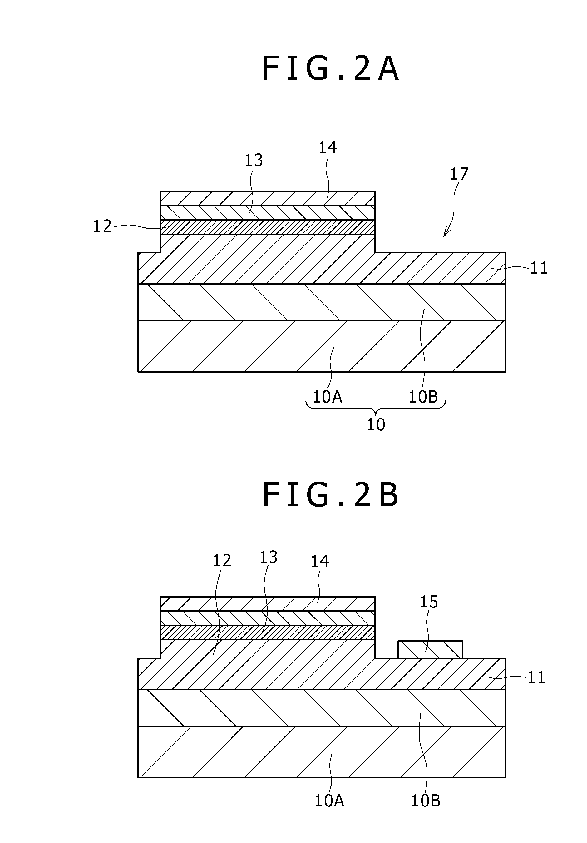
[0099]Example 3 is a modification of Example 1 or Example 2. In Example 3, a step of exposing the surface of the SOG layer 16 to a plasmaatmosphere is further provided between [Step 140] and [Step 150]. With the surface of the SOG layer 16 thus exposed to the plasmaatmosphere, organic matters (e.g., hydrocarbons) contained in the surface portion of the SOG layer 16 are removed, whereby an SOG layer 16 with high quality can be obtained. Examples of the conditions of the plasma atmosphere include the conditions shown in the following Table 1. Incidentally, the treatment of exposing the surface of the SOG layer 16 to a plasma atmosphere can similarly be carried out also in the following Examples.
TABLE 1Plasma atmosphere:O2 gas, Ar gas, N2 gas or the like,used either singly or in combinationPressure:0.1 to 100PaApplied power:350WTreating time:10min
CROSS REFERENCES TO RELATED APPLICATIONS[0001]The present invention contains subject matter related to Japanese Patent Application JP 2006-284051 filed in the Japan Patent Office on Oct. 18, 2006, the entire contents of which being incorporated herein by reference.BACKGROUND OF THE INVENTION[0002]1. Field of the Invention[0003]The present invention relates to a light emitting device and a method of manufacturing the same.[0004]2. Description of the Related Art[0005]A light emitting diode (LED) according to the related art, for example, one disclosed in Japanese Utility Model No. 3068914 has a light emitting layer having a stack structure in which, for example, an under layer 10B formed based on an MOCVD method, a first compound semiconductor layer 11 of a first conduction type (e.g., n-type), an active layer 12, and a second compound semiconductor layer 13 of a second conduction type (e.g., p-type) are stacked over a substrate 10A including, for example, sapphire, as shown in a sche...
Claims
Application Information
Patent Timeline
Application Date:The date an application was filed.
Publication Date:The date a patent or application was officially published.
First Publication Date:The earliest publication date of a patent with the same application number.
Issue Date:Publication date of the patent grant document.
PCT Entry Date:The Entry date of PCT National Phase.
Estimated Expiry Date:The statutory expiry date of a patent right according to the Patent Law, and it is the longest term of protection that the patent right can achieve without the termination of the patent right due to other reasons(Term extension factor has been taken into account ).
Invalid Date:Actual expiry date is based on effective date or publication date of legal transaction data of invalid patent.

