Monolithically integrated III-nitride power converter

a power converter and monolithic technology, applied in the field of monolithic integrated iiinitride power converters, novel integrated circuits, can solve the problems of undesired parasitics, difficult to integrate certain kinds of circuits, and long connections between power devices and their predrivers, so as to reduce parasitics, simplify the layout of devices, and reduce costs

Active Publication Date: 2008-06-12
INFINEON TECH AMERICAS CORP
View PDF6 Cites 114 Cited by
  • Summary
  • Abstract
  • Description
  • Claims
  • Application Information

AI Technical Summary

Benefits of technology

[0007]The closeness of the III-nitride-based power stage and the load reduces parasitic inductances due to long leads and wires (present in the prior art) and thus improves the overall performance of the circuit. In one variation, the III-nitride based power stage may use bumps (such as copper bumps) to be flip chip mounted to reduce or eliminate wirebonds, and thus further reduce parasitic resistance and inductance. For example, the power stage may be flip chip mounted on pads provided on the load or pads on a circuit board which is mounted on the load.
[0018]Substantial benefits are also obtained during fabrication of the predrivers with the power switches in that the predriver characteristics will be well matched, being subjected to the same oven temperatures, and deadtime is well optimized. Further, the trimming of the devices takes place at the same oven temperature.

Problems solved by technology

It is difficult to integrate certain kinds of circuits, for example, a buck converter circuit, which employs a power level synchronous MOSFET, a power level control MOSFET and the drivers therefor, especially in silicon because of device sizes and interconnections and the need for integrating high voltage and low voltage devices and their drivers in a single silicon die.
Because of layout limitations, the connections between power devices and their predrivers would be relatively long and non-linear, introducing undesired parasitics.

Method used


Image

  • Monolithically integrated III-nitride power converter
  • Monolithically integrated III-nitride power converter
  • Monolithically integrated III-nitride power converter

Examples


Embodiment Construction

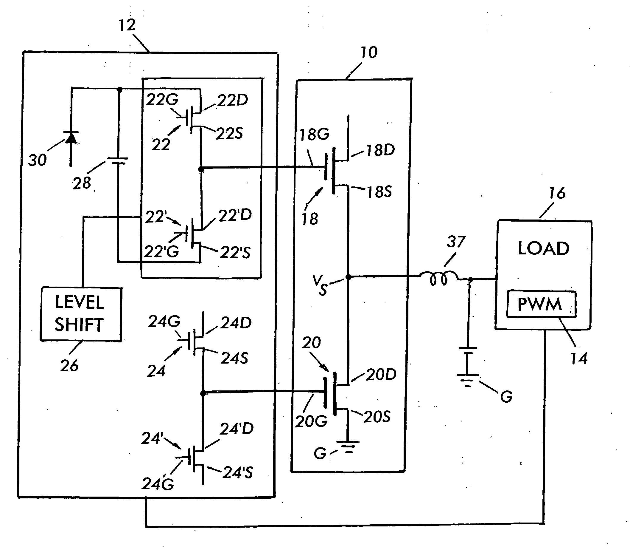
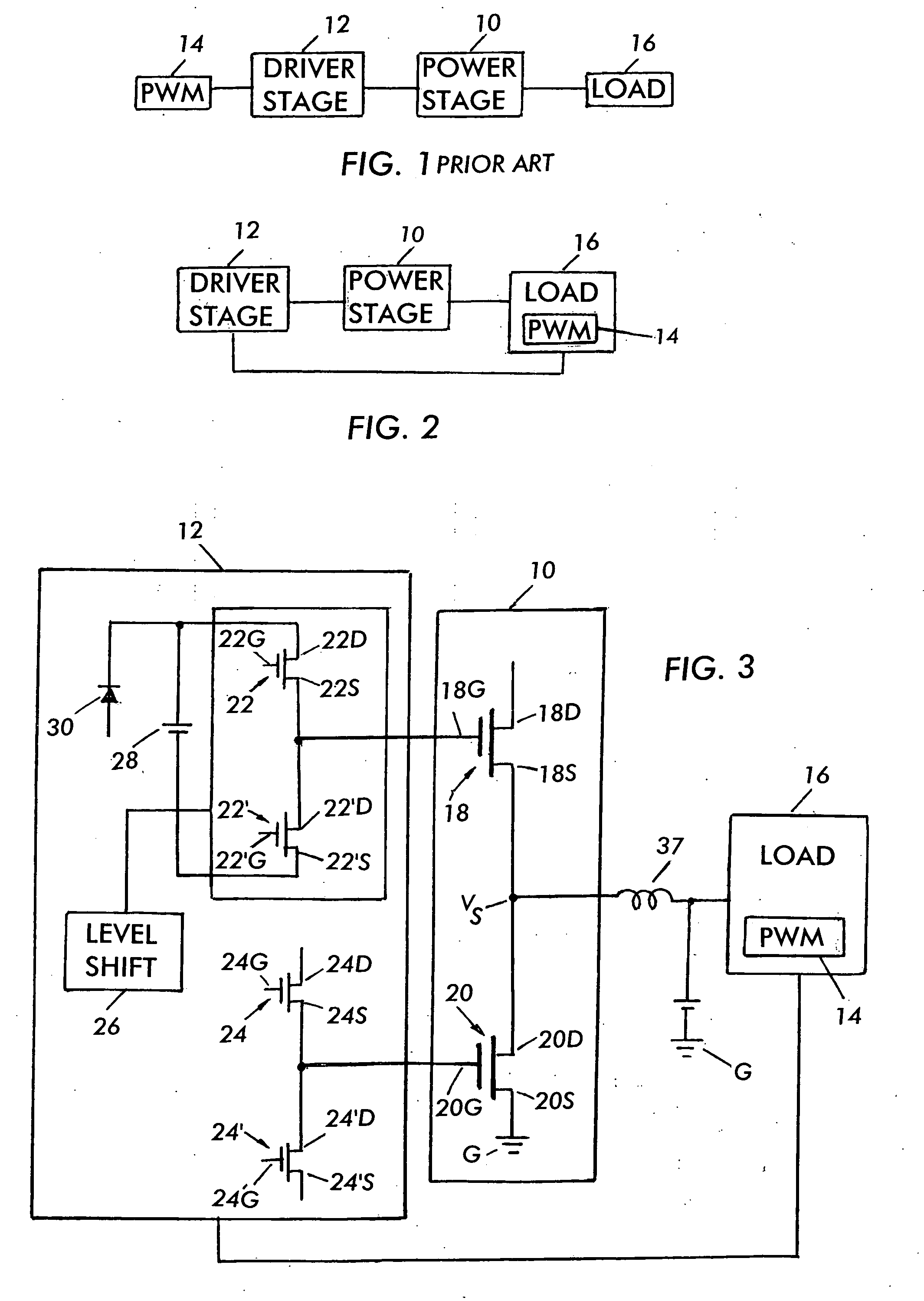
[0029]Referring to FIG. 1, a power management arrangement according to the prior art includes a power stage 10, a driver stage 12 operatively coupled to power stage 10 to control the operation of power stage 10, a pulse width modulation (PWM) stage 14 operatively coupled to driver stage 12 to control the operation thereof, and a load stage 16 operatively coupled to power stage 10 to receive power from the same.

[0030]In prior art arrangements, to maintain the proper supply of power to load stage 16, PWM stage 14 uses a predetermined criteria in order to operate driver stage 12. For example, a predetermined voltage level at the output of power stage 10 is used to determine whether driver stage 12 should operate power stage 10 to supply more power to load stage 16. In many designs, the predetermined value used for the operation of PWM 14 may not necessarily correspond to the instantaneous and transient requirements of load stage 16 which may surpass the predetermined value set forth fo...


PUM


Abstract

A power arrangement that includes a monolithically integrated III-nitride power stage having III-nitride power switches and III-nitride driver switches.

Description

RELATED APPLICATION[0001]This application is based on and claims priority to the of U.S. Provisional Application Ser. No. 60 / 874,411, filed on Dec. 11, 2006, entitled MONOLITHICALLY INTEGRATED GaN POWER CONVERTER, to which a claim of priority is hereby made and the disclosure of which is incorporated by reference.DEFINITION[0002]III-nitride device, including III-nitride power device, as called for herein refers to a semiconductor device that includes a III-nitride heterojunction having a conductive channel commonly referred to as a two-dimensional electron gas. The if III-nitride heterojunction would include two semiconductor bodies each being formed of a semiconductor alloy from the InAlGaN system.FIELD OF THE INVENTION[0003]This invention relates to semiconductor drivers and processes for their manufacture and more specifically relates to a novel integrated circuit employing plural III-nitride power devices and drivers therefor.BACKGROUND OF THE INVENTION[0004]Integrated circuits ...

Claims


Application Information

Patent Timeline
Patent Type & Authority Applications(United States)
IPC IPC(8): G05F1/00
CPCH01L27/0211H01L27/0605H01L29/2003H01L29/7787H01L21/8258H02M3/1588Y02B70/1466G05F1/10H02M3/155Y02B70/10G11C5/14G11C7/00
Inventor BRIERE, MICHAEL A.
Owner INFINEON TECH AMERICAS CORP
Why Eureka
Try Eureka