Polarizing element, method for manufacturing the same, liquid crystal device and electronic apparatus

a technology of polarizing elements and liquid crystal devices, which is applied in the direction of polarizing elements, instruments, applications, etc., can solve the problems of deterioration of optical characteristics of polarizing elements, and achieve the effects of fine optical characteristics, fine optical characteristics, and same optical characteristics

Inactive Publication Date: 2008-06-12
SEIKO EPSON CORP
View PDF11 Cites 18 Cited by
  • Summary
  • Abstract
  • Description
  • Claims
  • Application Information

AI Technical Summary

Benefits of technology

[0006]An advantage of the present invention is to provide a polarizing element having a coating film on the surface and fine optical characteristics, and to provide a manufacturing method thereof.
[0007]A polarizing element according to a first aspect of the invention includes a polarizing element member formed on a substrate and composed of a metal film that has a slit-shaped opening, the opening is provided in a plural number, a coating film formed on the polarizing element member and a space surrounded by the coating film, the substrate and the metal film. In this way, the polarizing element can have the same optical characteristics as those of a polarizing element in which the metal film forming the polarizing element member is released in the air.
[0008]A polarizing element according to a second aspect of the invention includes a polarizing element member formed on a substrate and composed of a metal film that has a slit-shaped opening, the opening is provided in a plural number, a coating film formed on the polarizing element member and an air layer formed in the opening. According to the second aspect, it is possible to realize the polarizing element having fine optical characteristics because the air layer is provided inside the opening. Alternatively, the opening can be filled with a predetermined gas (an argon gas, a nitrogen gas or the like) or the opening can be retained in vacuum state.
[0009]In these cases, it is preferable that an open end of the opening be closed by a part of the coating film which is an aggregation of crystal grains that grow from an upper face of the metal film toward a direction opposite to the metal film. In this way, the open end of the opening can be easily closed through the formation process of the coating film. Consequently, it is possible to simplify the manufacturing process of the polarizing element.
[0010]It is also preferable that a seed layer containing a constituent element of the coating film be formed on an upper face of the metal film, and the coating film be an aggregation of crystal grains that grow from the seed layer. By providing the seed layer that controls the crystal grains of the coating film, it is possible to control the growth of the crystal grains at ease. Accordingly, the open end of the opening can be efficiently blocked out at the time when the coating film is formed.
[0011]It is also preferable that the seed layer be selectively formed only on the upper face of the metal film. In this way, it is possible to prevent a part of the coating film from being formed on the side face of the metal film. Consequently, the coating film is hardly formed inside the opening in the polarizing element. This means that such polarizing element can acquire fine optical characteristics.

Problems solved by technology

However, if the protection film such as a silicon oxide film is formed directly on the polarizing element having the grid pattern made of an organic material, the optical characteristics of the polarizing element are largely deteriorated.

Method used


Image

  • Polarizing element, method for manufacturing the same, liquid crystal device and electronic apparatus
  • Polarizing element, method for manufacturing the same, liquid crystal device and electronic apparatus
  • Polarizing element, method for manufacturing the same, liquid crystal device and electronic apparatus

Examples


first embodiment

[0038]Polarizing Element

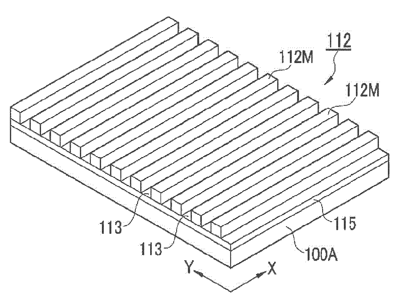
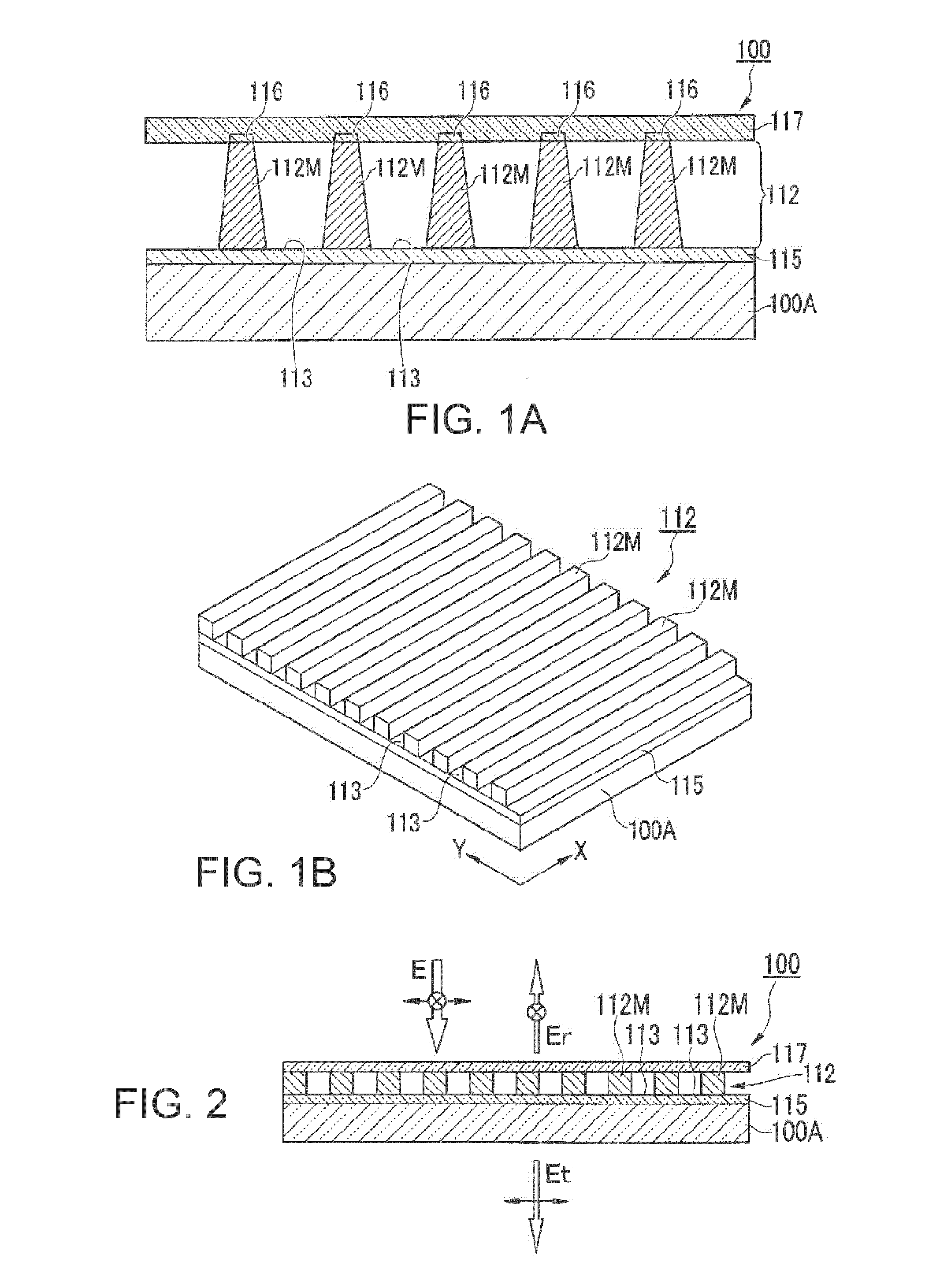
[0039]FIG. 1A is a partial sectional view of a polarizing element 100. FIG. 1B is a perspective view of a polarizing element member 112 forming the polarizing element 100. FIG. 2 is an explanatory drawing showing operation of the polarizing element 100.

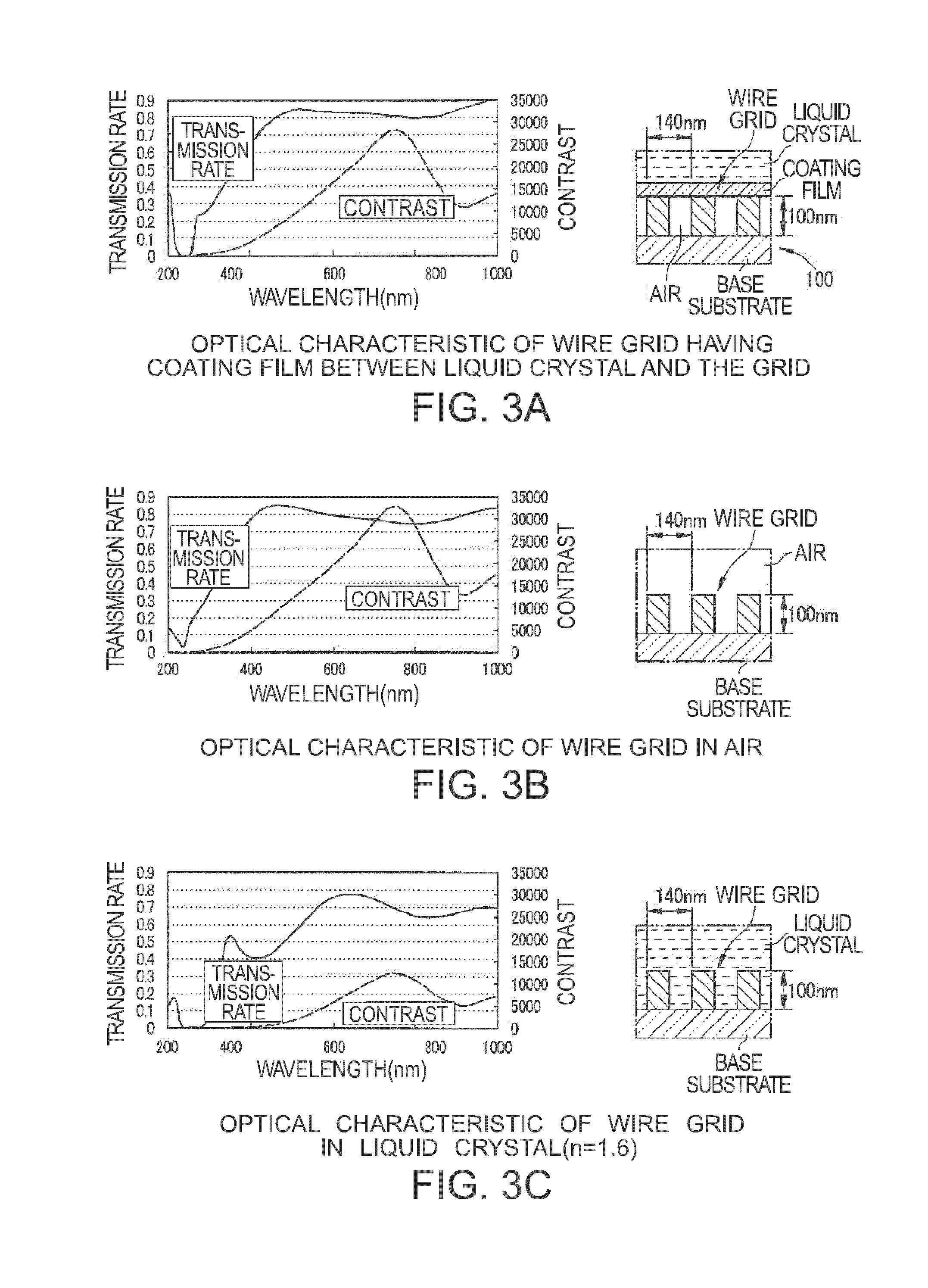
[0040]The polarizing element 100 is a light-reflective type polarizing element. The polarizing element 100 has a base layer 115 covering a base substrate 100A, the polarizing element member 112 formed on the base layer 115, and a coating film 117 formed on the polarizing element member 112. The polarizing element member 112 is mainly formed of a metal film 112M that is provided on the surface of the base layer 115 and has a slit-shaped opening 113 which is provided in the plural number. The polarizing element member 112 has a wire grid structure. The metal film 112M is patterned in a striped form when it is viewed in a planar direction. The strip has for example a width of 70 nm, a height of 100 nm and a pitch ...

second embodiment

[0073]A liquid crystal device having the polarizing element according to the invention as a reflective polarizing layer embedded therein is now described with reference to the accompanying drawings.

[0074]The liquid crystal device in this embodiment is a vertically aligned mode liquid crystal device in which the initial alignment is vertical and which has a liquid crystal layer having an anisotropic negative refractive index. The liquid crystal device in this embodiment is also a color liquid crystal device in which a color filter is provided on a substrate. A single pixel includes three sub-pixels that emit colored light beams of red (R), green (G) and blue (B) respectively. A minimum unit forming a display area is referred as a “sub-pixel region” and a set of the sub-pixels (R, G, B) is referred as a “pixel region”.

[0075]FIG. 7 is an equivalent circuit schematic of a plurality of the sub-pixel regions arranged in matrix in a liquid crystal device 200 according to the second embodim...

third embodiment

[0101]A liquid crystal device according to a third embodiment is now described with reference to the accompanying drawings. The liquid crystal device according to the third embodiment adopts a fringe field switching (FFS) method which is one of horizontal electric field methods in which the alignment is controlled by applying an electric field of the substrate face direction (horizontal direction) to the liquid crystal so as to display an image. The liquid crystal device according to the third embodiment is the color liquid crystal device having the color filter on the substrate.

[0102]FIG. 10 is a plan view of a single sub-pixel region in a liquid crystal device 300 according to the third embodiment. FIG. 11 is a sectional view of the sub-pixel region along the line B-B′ in FIG. 10.

[0103]A scale size of each layer or member in the drawings is appropriately set in order to make the layer or member recognizable. In the drawings which are referred in the following description, the iden...


PUM

PropertyMeasurementUnit
heightaaaaaaaaaa
heightaaaaaaaaaa
widthaaaaaaaaaa

Abstract

A polarizing element includes a polarizing element member formed on a substrate and composed of a metal film that has a slit-shaped opening, the opening being provided in a plural number, a coating film formed on the polarizing element member and a space surrounded by the coating film, the substrate and the metal film.

Description

BACKGROUND OF THE INVENTION[0001]1. Technical Field[0002]The present invention relates to a polarizing element, a method for manufacturing the same, a liquid crystal device and an electronic apparatus.[0003]2. Related Art[0004]A polarizing element is used in a light valve for a liquid crystal projector. In order to prevent deterioration under a high-temperature state and to increase light resistance of the polarizing element, Japanese Patent No. 3,654,553 (a first example) proposes a polarizing element having a grid pattern which is made of an organic material such as aluminum and formed on a glass substrate. JP-A-2002-520677 (a second example) proposes that such polarizing element be fitted in a liquid crystal device.[0005]According to the first example, a protection film and an insulating film are needed to be formed on the polarizing element in a case where the polarizing element made of an organic material is used as one of function elements forming the liquid crystal device. Es...

Claims


Application Information

Patent Timeline
Patent Type & Authority Applications(United States)
IPC IPC(8): G02F1/1335G02B5/30B44C1/22
CPCG02F2001/133548G02B5/3058G02F1/133548G02F1/1335
Inventor KUMAI, YOSHITOMO
Owner SEIKO EPSON CORP
Why Eureka
Try Eureka