
Encapsulated and water cooled electromagnet array

a technology of electromagnet array and encapsulation, which is applied in the direction of magnets, spray discharge apparatus, magnetic bodies, etc., can solve the problems of high aspect ratio, difficult to achieve, and sputter deposition into the deep and narrow via hol

Active Publication Date: 2008-06-19
APPLIED MATERIALS INC
View PDF3 Cites 20 Cited by
  • Summary
  • Abstract
  • Description
  • Claims
  • Application Information

AI Technical Summary

Benefits of technology

[0005]An array of multiple electromagnetic coils may be disposed as annular coils around the sidewalls of a plasma processing chamber to control the plasma. According to one aspect of the invention, the electromagnetic coils are encapsulated in a plastic to fix the coils with respect to each other. An advantageous configuration includes four electromagnetic coils in a rectangular array.

Problems solved by technology

However, sputter deposition into the deep and narrow via holes, that is, having a high aspect ratio, is difficult because sputtering is fundamentally a ballistical process with a nearly isotropic angular distribution pattern of sputtered ions. not immediately amenable to coating the sidewalls or even bottom of high aspect-ratio holes.
The uniformity of these ionized sputter processes, particularly when applied to 300 mm wafer in a reasonably sized sputter chamber, has presented further challenges.

Method used


Image

  • Encapsulated and water cooled electromagnet array
  • Encapsulated and water cooled electromagnet array
  • Encapsulated and water cooled electromagnet array

Examples


Embodiment Construction

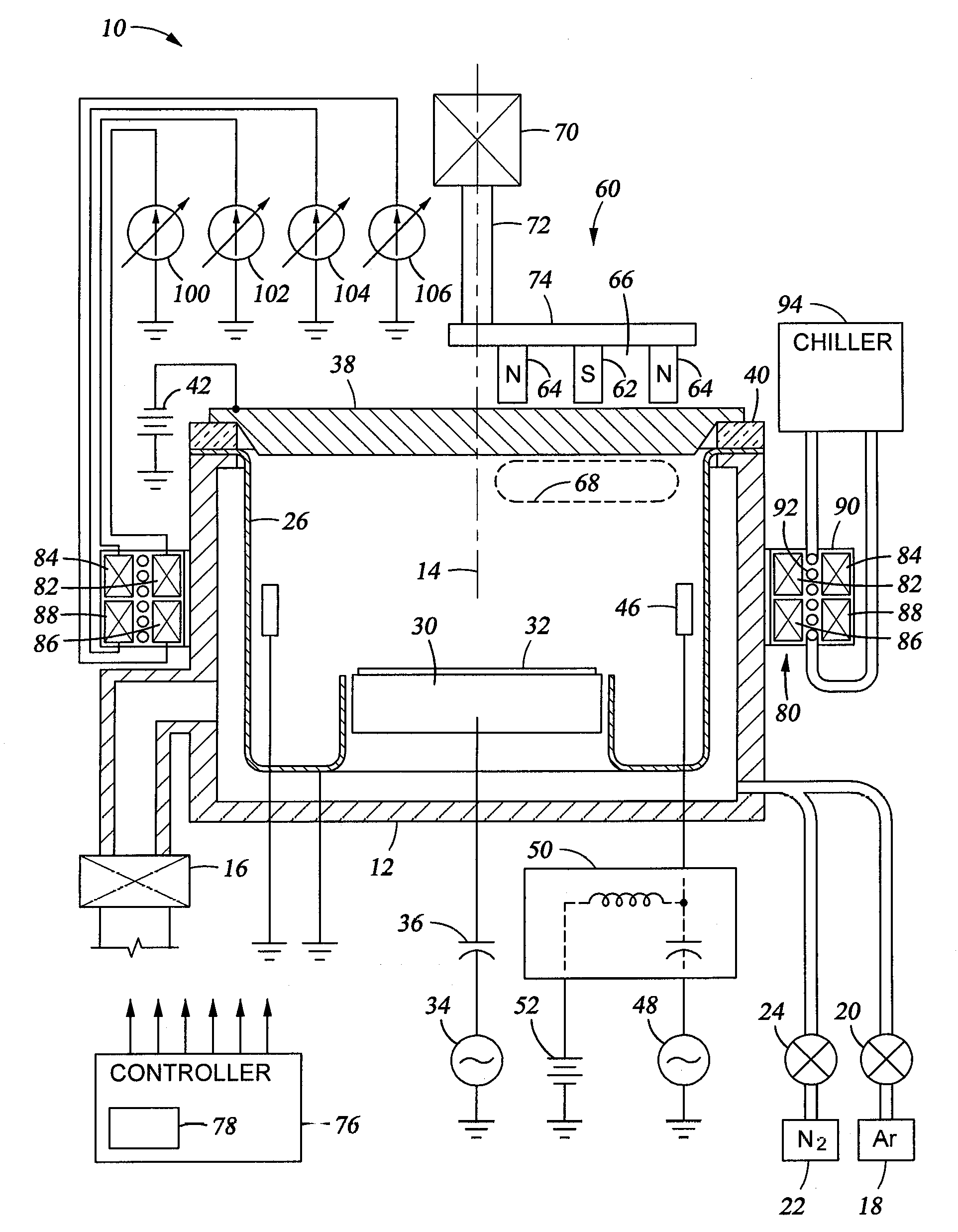
[0013]Gung et al. describe an advanced plasma sputter chamber in U.S. patent application Ser. No. 11 / 119,350, filed Apr. 29, 2005, now published as U.S. patent application Publication 2005 / 0263390, and incorporate herein by reference. The Gung chamber was developed for sputtering a refractory barrier layer, but we believe that a similar chamber can be used for sputtering copper seed layer as well as other materials.

[0014]Such a magnetron sputter chamber 10, schematically illustrated in cross section in FIG. 1, can effectively sputter thin films of Ta and TaN or alternatively Cu into holes having high aspect ratios and can further act to plasma clean the substrate and selectively etch portions of the deposited tantalum-based films. The sputter chamber 10 includes a vacuum chamber 12 arranged generally symmetrically about a central axis 14. A vacuum pump system 14 pumps the chamber 12 to a very low base pressure in the range of 10−6 Torr. However, a gas source 18 connected to the cham...


PUM

PropertyMeasurementUnit
pressureaaaaaaaaaa
angleaaaaaaaaaa
temperatureaaaaaaaaaa

Abstract

A electromagnet array structure including multiple electromagnetic coils captured in a rigid encapsulant, for example, of cured epoxy resin, to form a unitary free-standing structure which can be placed around the walls of a plasma processing chamber. A liquid cooling coil may also be captured in the encapsulant between the electromagnetic coils. The structure may additionally include water fittings, locating pins, through tubes for chamber bolts, and lifting brackets.

Description

FIELD OF THE INVENTION[0001]The invention relates generally to plasma processing of substrates. In particular, the relates to the RF coils and auxiliary magnets, for example, electromagnets used in a sputter reactor, most particularly in a multi-step process.BACKGROUND ART[0002]Sputtering, alternatively called physical vapor deposition (PVD), is used to deposit several different layers of metals and related materials in the fabrication of semiconductor integrated circuits. In two related and demanding application, first a thin barrier layer is sputtered onto the walls and bottom of a narrow hole etched into and often through an inter-level dielectric layer, most typically composed of silicon oxide or similar oxide materials. The barrier layer prevents the migration of metal into the oxide and oxygen into the metal filling the via hole. For copper metallization, the barrier layer is often composed of tantalum, for example, a bilayer of Ta / TaN. Then a thin seed layer of copper is depo...

Claims


Application Information

Patent Timeline
Patent Type & Authority Applications(United States)
IPC IPC(8): C23C16/513H01F41/04H01F7/20
CPCH01F7/128H01F7/20H01F27/16Y10T29/4902H01J37/3266H01J37/3458H01J37/347H01J37/32623
Inventor GILLARD, ANDREWVESCI, ANTHONYMILLER, KEITH A.
Owner APPLIED MATERIALS INC
Features
  • Generate Ideas
  • Intellectual Property
  • Life Sciences
  • Materials
  • Tech Scout
  • Unparalleled Data Quality
  • Higher Quality Content
  • 60% Fewer Hallucinations
Learn More