Method of fabricating a trench capacitor having increased capacitance

a trench capacitor and capacitor technology, applied in the direction of semiconductor devices, electrical equipment, transistors, etc., can solve the problems of increasing the difficulty of etching deep trenches into silicon substrates, difficult to ascertain capacitance, and reducing the geometries of memory cells, so as to achieve the effect of higher capacitan

Inactive Publication Date: 2008-06-19
NAN YA TECH
View PDF20 Cites 9 Cited by
  • Summary
  • Abstract
  • Description
  • Claims
  • Application Information

AI Technical Summary

Benefits of technology

[0010]It is the primary object of the present invention to provide an improved method of fabricating a trench capacitor and trench capacitor DRAM device at very small line width such as 90 nm or below, thereby overcoming the limit of the trench etching techniques and obtaining higher capacitance.

Problems solved by technology

DRAM technology faces enormous challenges when reducing the memory cell geometries.
When there is a shortage of capacitance, the information of charges stored in the capacitor is not easily detected, which results in making the capacitance difficult to ascertain.
However, etching deep trench into the silicon substrate become more and more difficult as the aspect ratio of the deep trench gets larger.
The conventional trench etching and trench fill technology has almost reached its limit.

Method used


Image

  • Method of fabricating a trench capacitor having increased capacitance
  • Method of fabricating a trench capacitor having increased capacitance
  • Method of fabricating a trench capacitor having increased capacitance

Examples


Embodiment Construction

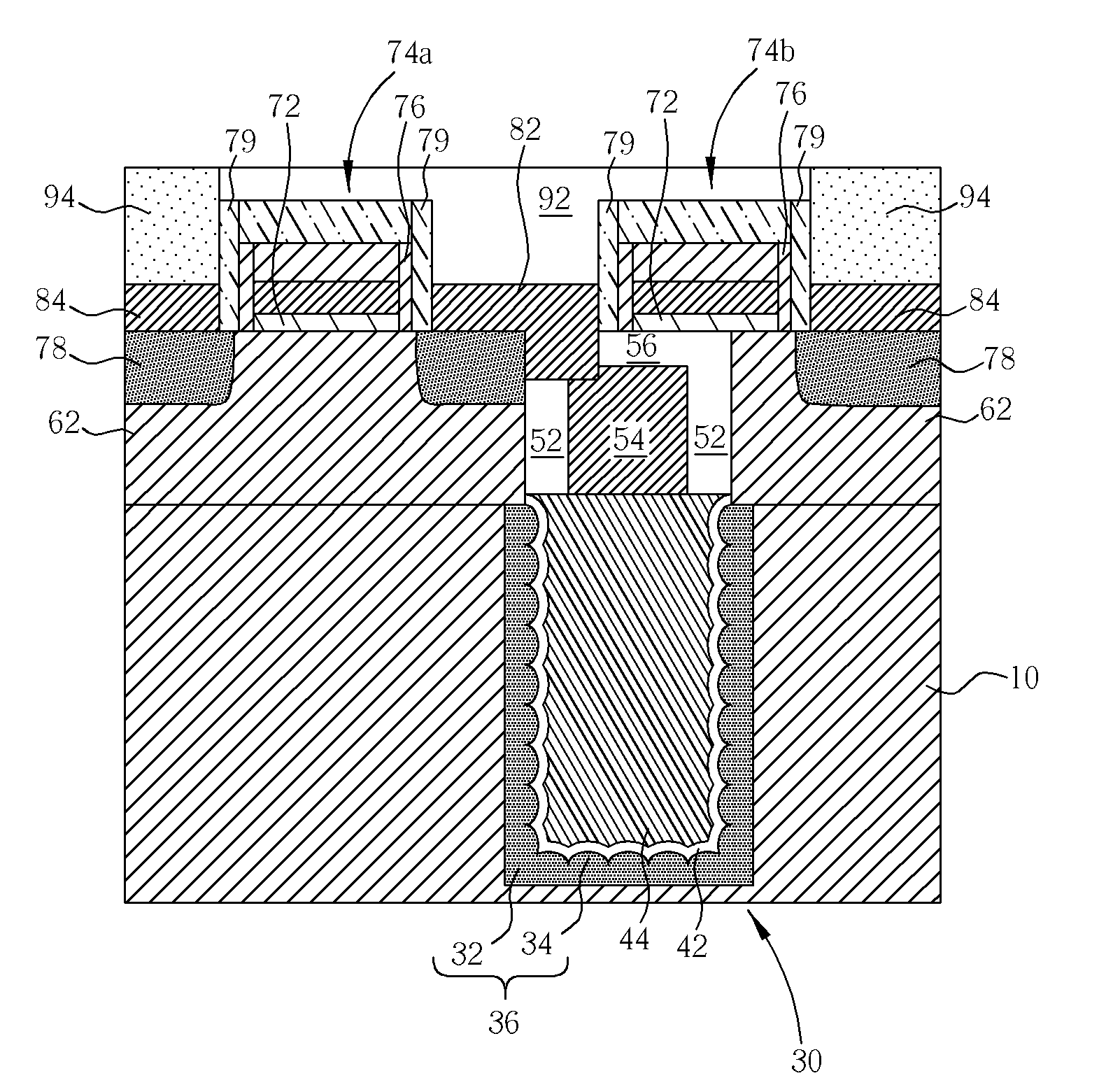
[0045]The present invention pertains to a method of fabricating a trench capacitor of DRAM devices having increased capacitance. To tackle a difficult problem of etching deeper trenches having a high aspect ratio, an epitaxial silicon growth process is employed in the fabrication of next-generation trench DRAM devices. A large-capacitance trench capacitor is first fabricated in the silicon substrate. An epitaxial silicon layer is then grown on the silicon substrate. Active areas, shallow trench isolation regions, and gate conductors are formed on / in the epitaxial silicon layer.

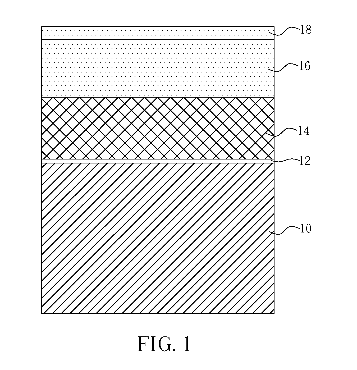
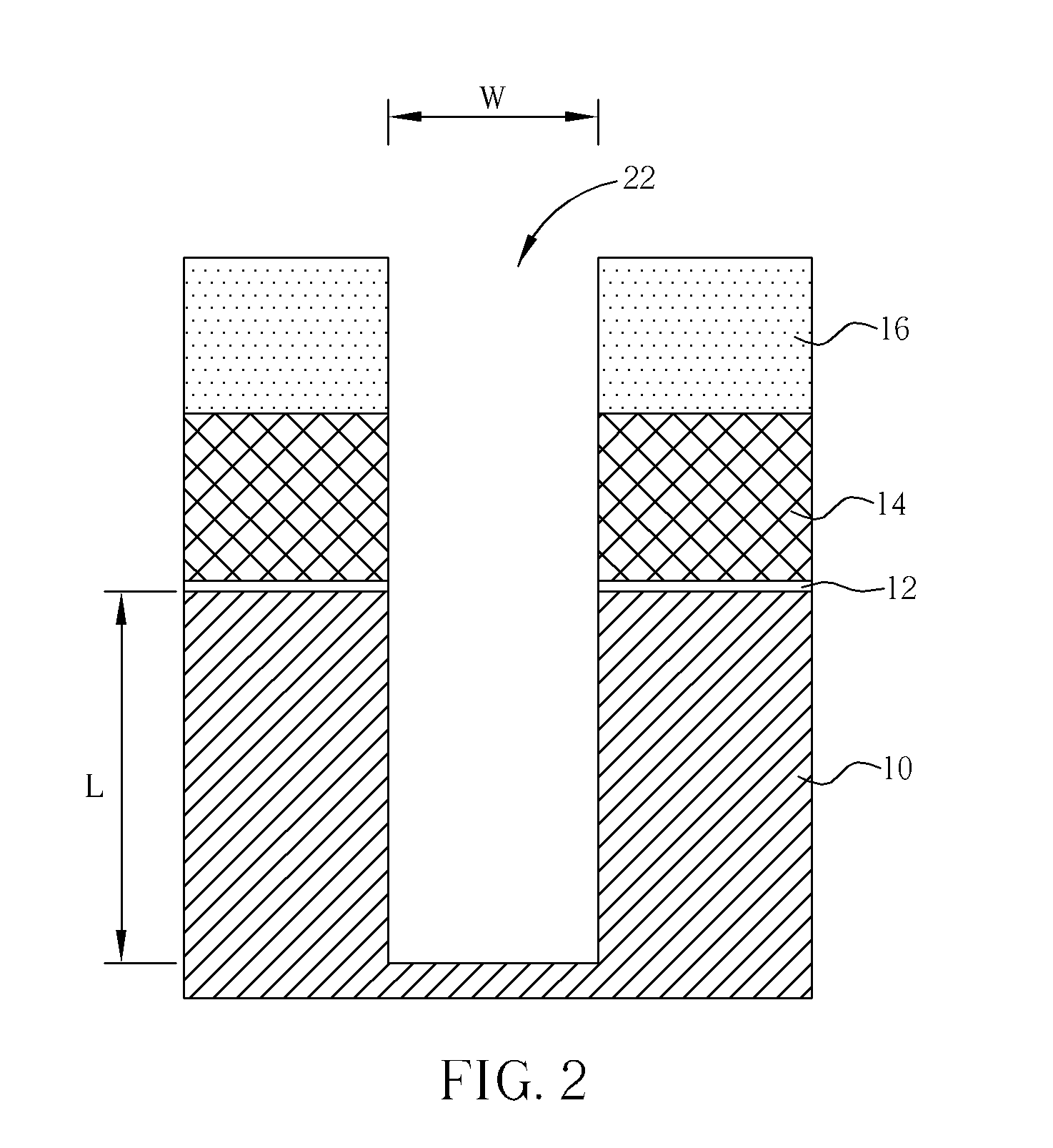
[0046]Please refer to FIG. 1 to FIG. 14. FIGS. 1-14 are schematic, cross-sectional diagrams illustrating the process of fabricating a deep trench capacitor of a DRAM device in accordance with one preferred embodiment of this invention. As shown in FIG. 1, a pad oxide layer 12 of about 30 angstroms, a pad nitride layer 14 of about 5000-5500 angstroms, a boron silicate glass (BSG) layer 16 of about 1.5-1.8 micro...


PUM

PropertyMeasurementUnit
thicknessaaaaaaaaaa
thicknessaaaaaaaaaa
depthaaaaaaaaaa

Abstract

The present invention pertains to a method of fabricating a trench capacitor having increased capacitance. To tackle a difficult problem of etching deeper trenches having very high aspect ratio, an epitaxial silicon growth process is employed in the fabrication of next-generation trench DRAM devices. A large-capacitance trench capacitor is first fabricated in the silicon substrate. An epitaxial silicon layer is then grown on the silicon substrate. Active areas, shallow trench isolation regions, and gate conductors are formed on / in the epitaxial silicon layer.

Description

CROSS REFERENCE TO RELATED APPLICATIONS[0001]This patent application is a divisional application of co-pending U.S. patent application Ser. No. 11 / 466,105, filed on Aug. 22, 2006 and titled “METHOD OF FABRICATING A TRENCH CAPACITOR HAVING INCREASED CAPACITANCE.” The entire contents of which are incorporated herein by reference.BACKGROUND OF THE INVENTION[0002]1. Field of the Invention[0003]The present invention relates generally to the field of semiconductor fabrication and, more particularly, to an improved method of fabricating a trench capacitor structure of dynamic random access memory (DRAM) devices.[0004]2. Description of the Prior Art[0005]Along with the development of miniaturization of various electrical products, DRAM elements have been pushed for size reductions to match the trends toward high integration and high density. DRAM technology faces enormous challenges when reducing the memory cell geometries.[0006]As the line width of fabricating processes is reduced to 0.11 ...

Claims


Application Information

Patent Timeline
Patent Type & Authority Applications(United States)
IPC IPC(8): H01L29/94
CPCH01L29/66181H01L27/1087H10B12/0387
Inventor LIAO, SAMCHEN, MENG-HUNGLIAO, HUNG-CHANG
Owner NAN YA TECH
Why Eureka
Try Eureka