Nanostructure Having a Nitride-Based Quantum Well and Light Emitting Diode Employing the Same

a quantum well and nanostructure technology, applied in the field of nanostructures and light-emitting diodes, can solve the problems of limited performance, temperature sensitivity, low light-emitting efficiency, and large deviation of output, and achieve high light-emission efficiency, reduce the influence of non-radiative recombination, and high luminance

Active Publication Date: 2008-07-03
SEOUL VIOSYS CO LTD
View PDF14 Cites 65 Cited by
  • Summary
  • Abstract
  • Description
  • Claims
  • Application Information

AI Technical Summary

Benefits of technology

[0006]An object of the present invention is to provide a nanostructure with high luminance and high light-emission efficiency, which can reduce the influence of non-radiative recombination on a surface of the nanostructure.
[0007]Another object of the present invention is to provide a light emitting diode employing an array of nanostructures capable of reducing the influence of non-radiative recombination on surfaces of the nanostructures.
[0008]A further object of the present invention is to provide a method of fabricating a light emitting diode employing an array of nanostructures capable of reducing the influence of non-radiative recombination on surfaces of the nanostructures.Technical Solution
[0009]To achieve the objects of the present invention, the present invention provides a nanostructure, a light emitting diode employing the nanostructure, and a method of fabricating the light emitting diode. According to an aspect of the present invention, the nanostructure includes a core nanorod having a first nanorod of a first conductivity type, a (AlxInyGa1-x-y)N (where, 0≦x<1, 0≦y≦1 and 0≦x+y≦1) quantum well, and a second nanorod of a second conductivity type, which are joined in a longitudinal direction. A nano shell formed of a material with a bandgap greater than that of the quantum well surrounds at least the quantum well. According to the aspect of the present invention, it is possible to provide an LED having a nanostructure with high luminance and high light-emission efficiency by interposing the (AlxInyGa1-x-y)N quantum well between the p-n junction interface. It is also possible to further improve the light-emission efficiency by reducing non-radiative recombination on a surface of the quantum well by means of the nano shell.
[0014]In addition, at least two of the plurality of (AlxInyGa1-x-y)N (where, 0≦x<1, 0≦y≦1 and 0≦x+y≦1) layers may have different amounts of In and / or different thicknesses. As the amount of In increases, the bandgap of (AlxInyGa1-x-y)N decreases. Accordingly, it is possible to implement light with at least two peak wavelengths, e.g., multi-color light, by adjusting the amounts of In in the (AlxInyGa1-x-y)N layers. Further, the bandgap of the (AlxInyGa1-x-y)N layer increases by reducing the thickness of the (AlxInyGa1-x-y)N layer to the Bohr excitation radius or less. Thus, it is possible to implement light with at least two peak wavelengths, e.g., multi-color light, by adjusting the thicknesses of the (AlxInyGa1-x-y)N layers.

Problems solved by technology

A typical GaN LED, i.e., a laminated-film type LED formed by sequentially stacking an n-type impurity-doped n-GaN layer, an InGaN active layer, and a p-type impurity-doped p-GaN layer on a sapphire substrate, has limited performance (luminance), because there are a great deal of threading dislocations caused by lattice mismatching due to physical properties or limitations on growth of GaN.
A laminated-film GaN LED has advantages in that it is relatively easy to design and fabricate and has low temperature sensitivity, while it has disadvantages of a low efficiency of light emitting, a wide spectrum width, a high output deviation and the like, as well as the threading dislocations.
Since the nanorod-structured LED is a simple p-n junction diode, it is difficult to obtain high luminance.
In a photolithography and etching process, however, the lattice structure of GaN is damaged.
This makes the luminance or light-emission efficiency of a product unsatisfactory.
Meanwhile, since a nanorod LED has a great ratio of surface to volume, non-radiative recombination on a surface greatly affects external quantum efficiency of the nanorod LED.

Method used


Image

  • Nanostructure Having a Nitride-Based Quantum Well and Light Emitting Diode Employing the Same
  • Nanostructure Having a Nitride-Based Quantum Well and Light Emitting Diode Employing the Same
  • Nanostructure Having a Nitride-Based Quantum Well and Light Emitting Diode Employing the Same

Examples


Embodiment Construction

[0029]Hereinafter, preferred embodiments of the present invention will be described in detail with reference to the accompanying drawings. The following embodiments are provided only for illustrative purposes so that those skilled in the art can fully understand the spirit of the present invention. Therefore, the present invention is not limited to the following embodiments but may be implemented in other forms. In the drawings, the widths, lengths, thicknesses and the like of elements are exaggerated for convenience of illustration. Like reference numerals indicate like elements throughout the specification and drawings.

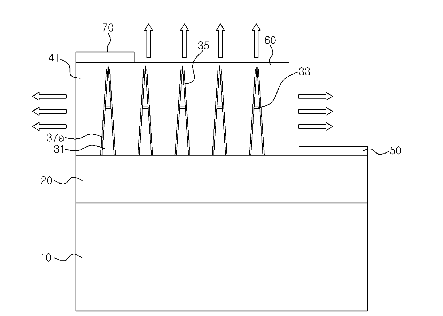
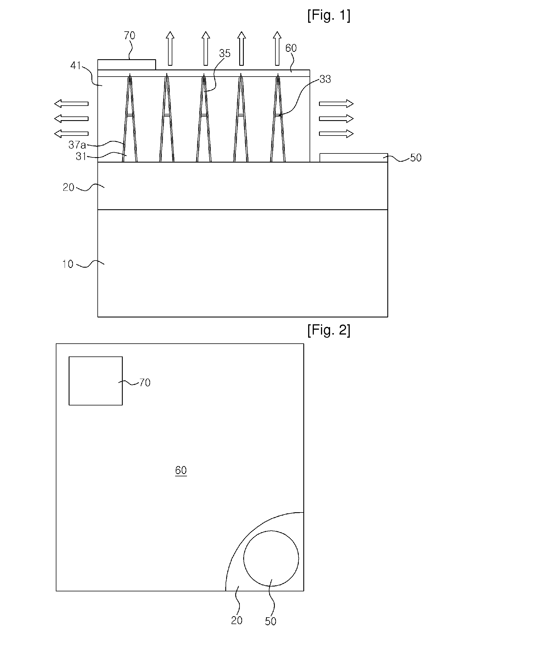
[0030]FIG. 1 is a sectional view of a light emitting diode (hereinafter, referred to as LED) according to an embodiment of the present invention, and FIG. 2 is a plan view of the light emitting diode shown in FIG. 1.

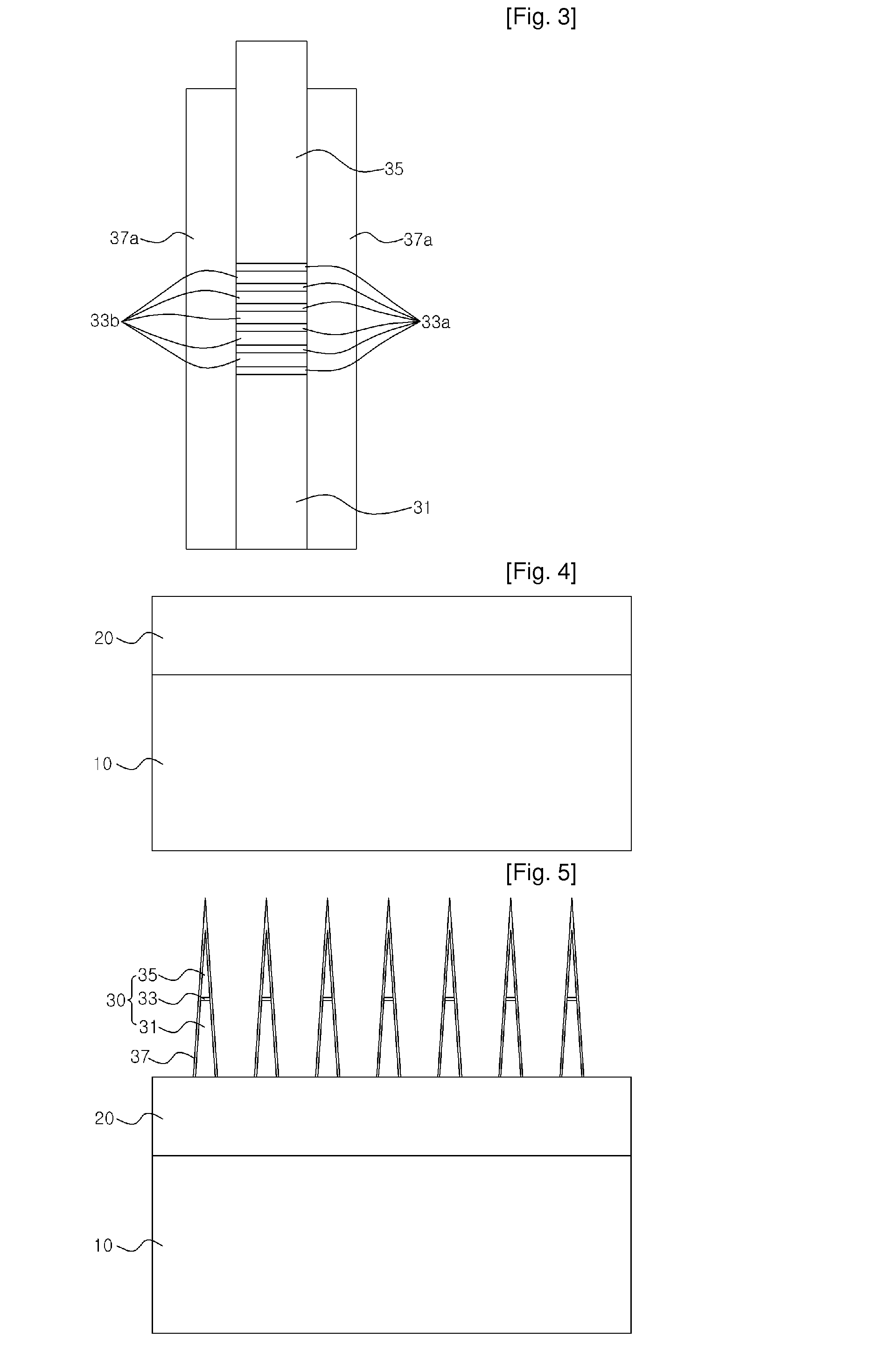
[0031]Referring to FIGS. 1 and 2, the light emitting diode comprises an array of nanostructures on a substrate 10. The substrate 10 may be an insulating...


PUM

PropertyMeasurementUnit
peak wavelengthaaaaaaaaaa
temperatureaaaaaaaaaa

Abstract

Disclosed are a nanostructure with an indium gallium nitride quantum well and a light emitting diode employing the same. The light emitting diode comprises a substrate, a transparent electrode and an array of nanostructures interposed between the substrate and the transparent electrode. Each of the nanostructures comprises a core nanorod, and a nano shell surrounding the core nanorod. The core nanorod is formed substantially perpendicularly to the substrate and includes a first nanorod of a first conductivity type, an (AlxInyGa1-x-y)N (where, 0≦x≦1, 0≦y≦1 and 0≦x+y≦1) quantum well, and a second nanorod of a second conductivity type, which are joined in a longitudinal direction. The nano shell is formed of a material with a bandgap greater than that of the quantum well, and surrounds at least the quantum well of the core nanorod. Meanwhile, the second nanorods are connected in common to the transparent electrode. Accordingly, with the nano shells, it is possible to provide a light emitting diode capable of improving external quantum efficiency by preventing non-radiative recombination on a surface of the (AlxInyGa1-x-y)N quantum well.

Description

TECHNICAL FIELD[0001]The present invention relates to a nanostructure, a light emitting diode employing the same, and a method of fabricating the same, and more particularly, to a nanostructure having a nitride-based quantum well, a light emitting diode employing an array of the nanostructures, and a method of fabricating the same.BACKGROUND ART[0002]Initially, an LED has been widely used as a simple display element for an instrument panel. In recent years, the LED attracts attention as a full color display device with high luminance, high visibility and long life cycle, such as a large-sized electronic display board, and light sources for backlight and general illumination. This is achieved through recent development of blue and green LEDs with high luminance. Meanwhile, a III-nitrogen compound semiconductor such as GaN is recently studied as a material for LEDs. This is because a III-V group nitride semiconductor has wide bandgap and thus enables obtainment of light in a substanti...

Claims


Application Information

Patent Timeline
Patent Type & Authority Applications(United States)
IPC IPC(8): H01L33/00H01L29/15H01L33/06H01L33/12H01L33/32H01L33/50
CPCB82Y20/00H01L33/06H01L33/32H01L33/18H01L33/08B82B3/00
Inventor KIM, HWA MOK
Owner SEOUL VIOSYS CO LTD
Why Eureka
Try Eureka