Plasma Processing Apparatus And Method Of Producing Semiconductor Thin Film Using The Same

a technology of plasma processing and semiconductor thin film, which is applied in the direction of electrolysis components, vacuum evaporation coatings, coatings, etc., can solve the problems of large chamber size, high cost of each constituent member, and affecting the size of the chamber, so as to reduce the cost, simplify the whole apparatus structure, and alleviate the effect of temperature ris

Inactive Publication Date: 2008-07-10
SHARP KK
View PDF7 Cites 5 Cited by
  • Summary
  • Abstract
  • Description
  • Claims
  • Application Information

AI Technical Summary

Benefits of technology

[0040]In the plasma processing apparatus of the present invention, the cathode, the anode, and the heater are spaced apart from the wall surface of the chamber and supported by the inside structural body, so that there is no need of reinforcement against the atmospheric pressure, leading to simplification of the whole structure of the apparatus and thereby further realizing the lowering of costs.
[0041]Also, since the plasma processing apparatus of the present invention is provided with heat-dissipating means for alleviating the temperature rise caused by the Joule heat generated in plasma discharging, the process can be stabilized by stabilizing the temperature during the plasma processing, whereby a good film having a uniform film quality and film thickness can be formed.
[0042]Further, the heat conductance to the outside of the apparatus is restrained by the heat-dissipating means, and the cooling apparatus on the outer wall surface of the chamber can be omitted, leading to simplification of the apparatus and thereby further realizing the lowering of costs.
[0043]Also, according to the method of producing a semiconductor thin film of the present invention, a semiconductor element using a semiconductor thin film or an optical thin film, such as a solar cell, a TFT, or a photo conductor, can be produced at a lower cost and with a good efficiency.

Problems solved by technology

However, since the cathode and the anode are used also as the wall surface of the chamber that is affected by the outside atmospheric pressure, the apparatus as a whole will be a large structural body, so that each constituent member will be expensive, and a cooling apparatus (cooling section) for cooling from the rear surface side of the chamber will be needed.
Therefore, in introducing electric power, it is difficult to ensure a grounding distance to the wall surface, so that the plasma discharge also is liable to be affected by the wall surface and others.
If this is carried out, the size of the chamber will have a large scale, thereby giving a factor for great increase in the costs.
For this reason, a large-scale insulating member will be needed, thereby giving a factor for great increase in the costs.
(F) When a fluorine-based etching gas is used as the reactive gas, an expensive fluorine-based rubber sealing material must be used for the vacuum sealing section of the cathode and the vacuum sealing sections of the anode near the plasma discharge region, thereby giving a factor for great increase in the costs.
(G) Since the gas exhausting outlet is disposed in one direction around the plasma discharge region, the conductance of the reactive gas will be small, making it difficult to perform exchange of a large amount of gas.
(I) In the case of a longitudinal-type plasma processing apparatus, the substrate is fixed in the surroundings, thereby raising a fear of insufficient grounding.
However, this apparatus is not provided with a mechanism that can fully alleviate the heat generation by the plasma that is generated in film forming or cleaning (etching), thereby raising a fear of inviting a large obstacle against the stability of the process.

Method used


Image

  • Plasma Processing Apparatus And Method Of Producing Semiconductor Thin Film Using The Same
  • Plasma Processing Apparatus And Method Of Producing Semiconductor Thin Film Using The Same
  • Plasma Processing Apparatus And Method Of Producing Semiconductor Thin Film Using The Same

Examples


embodiment 1

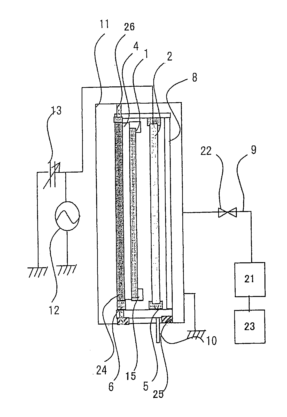
[0090]FIG. 1 is (a) a schematic cross-sectional view showing a longitudinal structure and (b) a schematic plan view showing a planar structure, of the plasma processing apparatus of Embodiment 1.

[0091]The chamber 11 is preferably made of a material having a strength as a vacuum vessel and being provided with heat conductivity and heat resistance, and is made of stainless steel, aluminum alloy, or the like.

[0092]The chamber 11 is constructed in such a manner that the inside thereof can be controlled to have an arbitrary vacuum degree. For this reason, the engagement part of the chamber 11 is completely sealed with an O-ring or the like. Also, a pressure controller 22 and a vacuum pump 21 are connected to the chamber 11 via a gas exhausting pipe 9, and a removing apparatus 23 for removing harmful substances within the exhaust gas after reaction of the reactive gas introduced into the chamber 11 is connected to the vacuum pump 21.

[0093]A holding leg 25 having a sufficient strength capa...

embodiment 2

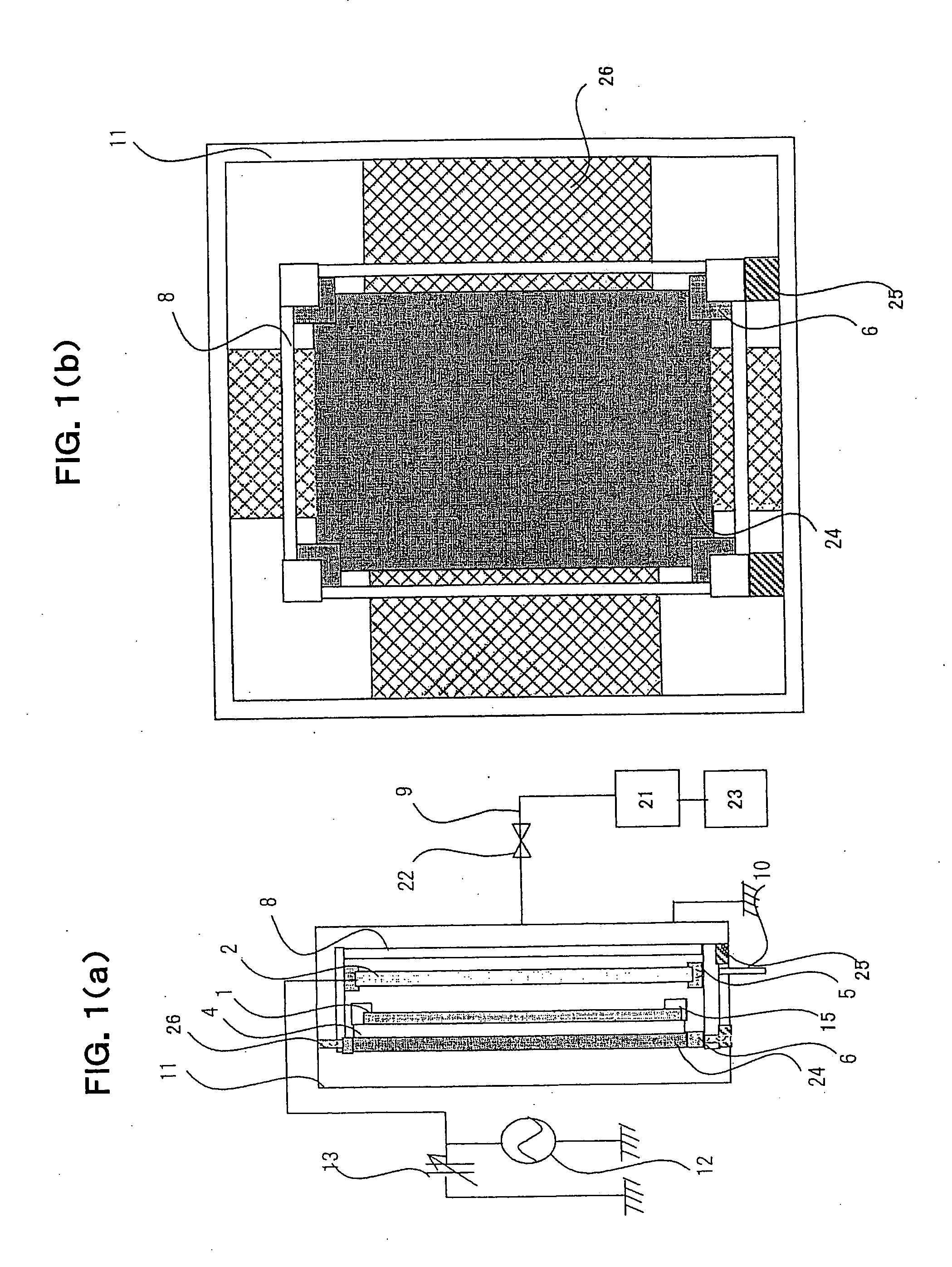
[0123]FIG. 2 is (a) a schematic cross-sectional view showing a longitudinal structure and (b) a schematic plan view showing a planar structure, of the plasma processing apparatus of Embodiment 2.

[0124]The structure of the plasma processing apparatus of Embodiment 2 is similar to that of Embodiment 1 except for the structure of the heat-dissipating means, so that mainly the different points will be described. Here, in FIG. 2, constituent elements similar to those of FIG. 1 are denoted with the same symbols.

[0125]The anode 4 has a dimension similar to that of Embodiment 1, and incorporates a heater 24.

[0126]Also, to the back surface of the heater 24, plural sheets of a heat-dissipating fin 27 are connected. Namely, the heat-dissipating fin 27 is disposed on the outer wall surface of the inside structural body on the substrate side. Here, in FIG. 2, the heat-dissipating fin 27 is not in contact with the chamber 11; however, it may be in contact as well.

[0127]This heat-dissipating fin 2...

embodiment 3

[0141]FIG. 4(a) is a schematic cross-sectional view showing a longitudinal structure of the plasma processing apparatus of Embodiment 3-1, and FIG. 4(b) is a schematic cross-sectional view showing a longitudinal structure of the plasma processing apparatus of Embodiment 3-2.

[0142]Also, FIG. 5 is a schematic view showing a structure of an air-cooled gas passing pipe 7 disposed in the heater in the plasma processing apparatus of Embodiment 3, where FIG. 5(a) is a view as viewed from the side-surface side, and FIG. 5(b) is a view as viewed from the plane side.

[0143]The structure of the plasma processing apparatus of Embodiment 3 is similar to that of Embodiment 1 except for the structure of the heat-dissipating means, so that mainly the different points will be described. Here, in FIGS. 4 and 5, constituent elements similar to those of FIG. 1 are denoted with the same symbols.

[0144]The anode 4 incorporates a heater 24 with a dimension similar to that of Embodiment 1. For example, as sh...


PUM

PropertyMeasurementUnit
constant temperatureaaaaaaaaaa
temperatureaaaaaaaaaa
sizeaaaaaaaaaa

Abstract

A plasma processing apparatus characterized by comprising within a sealable chamber: an internal structural body that is disposed to be spaced apart from an inner wall surface of the chamber and that forms an inside space for housing a substrate serving as an object of processing; a substrate holding section that houses the substrate within the inside space; reactive gas supplying means for supplying a reactive gas to the inside space; a cathode and an anode that are supported by the internal structural body and disposed on both sides of the substrate within the inside space and that generate plasma discharge of the reactive gas; a heater that is supported by the internal structural body and that heats the substrate within the inside space; and heat-dissipating means capable of dissipating a Joule heat generated by the plasma discharge to outside of the inside space.

Description

TECHNICAL FIELD[0001]The present invention relates to a plasma processing apparatus that performs etching or film-forming on a substrate by plasma discharge of a reactive gas as well as a method of producing a semiconductor thin film using the same.BACKGROUND ART[0002]Plasma processing apparatus are often used in producing a semiconductor element, and those having various forms are adapted for practical use in accordance with an object thereof.[0003]FIG. 6 is a schematic cross-sectional view of a conventional general longitudinal-type plasma processing apparatus.[0004]This plasma processing apparatus includes a chamber 11 that becomes a reaction vessel by receiving influence of outside atmospheric pressure. On the inner wall surface of the chamber 11, a cathode 2 and an anode 4 that are opposing to each other for causing plasma discharge, and a heater 24 that heats a substrate 1 (for example, a glass substrate) serving as an object of processing are disposed. Here, the heater 24 is ...

Claims


Application Information

Patent Timeline
Patent Type & Authority Applications(United States)
IPC IPC(8): C23C14/32
CPCH01J37/32009H01J37/32522H01L21/67103H01L21/3065H01J2237/2001
Inventor KISHIMOTO, KATSUSHIFUKUOKA, YUSUKE
Owner SHARP KK
Why Eureka
Try Eureka