Low resistance high-tmr magnetic tunnel junction and process for fabrication thereof

a high-tmr, magnetic tunnel junction technology, applied in the field of magnetic based sensors, can solve the problems of high current and power requirements to make a functional memory device or cell, etc., to achieve the effect of high electrical resistance, reducing the resistivity of the barrier layer, and accelerating the associated switching

Active Publication Date: 2008-07-10
AVALANCHE TECH
View PDF99 Cites 94 Cited by
  • Summary
  • Abstract
  • Description
  • Claims
  • Application Information

AI Technical Summary

Benefits of technology

[0012]Of the several layers in a memory element, the barrier layer typically has the highest electrical resistance. By reducing the resistivity of the barrier layer, the memory element's electrical resistivity, and the associated switching is accelerated especially in a memory array where voltage across the memory element depends on the size of the transistor, which advantageously increases scalability of such memory device having multiple memory elements. The reduction in resistance is achiev

Problems solved by technology

Prevalent media include rotating magnetic media, such as hard disk drives (HDDs) for non-volatile storage, or dynamic random access memory (DRAM) and static RAM (SRAM), which are volatile and very costly but have fast random read/write access time.
One of the problems with prior art memory structures is that the current and power requirements are too high to make a functional memory devi

Method used


Image

  • Low resistance high-tmr magnetic tunnel junction and process for fabrication thereof
  • Low resistance high-tmr magnetic tunnel junction and process for fabrication thereof
  • Low resistance high-tmr magnetic tunnel junction and process for fabrication thereof

Examples


Embodiment Construction

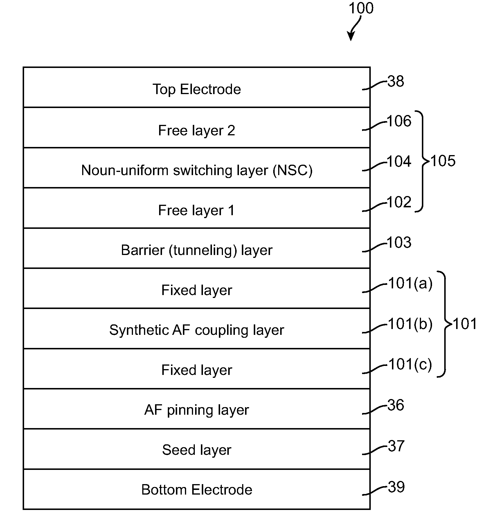
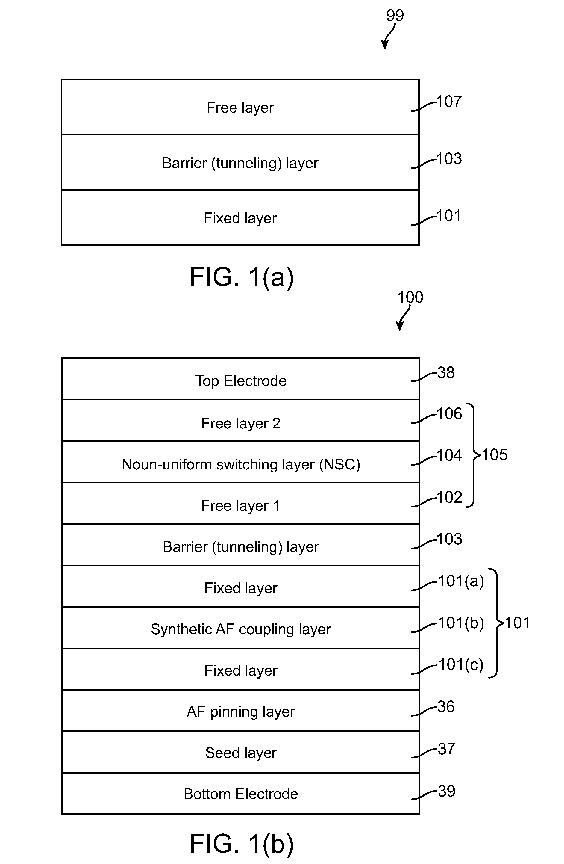
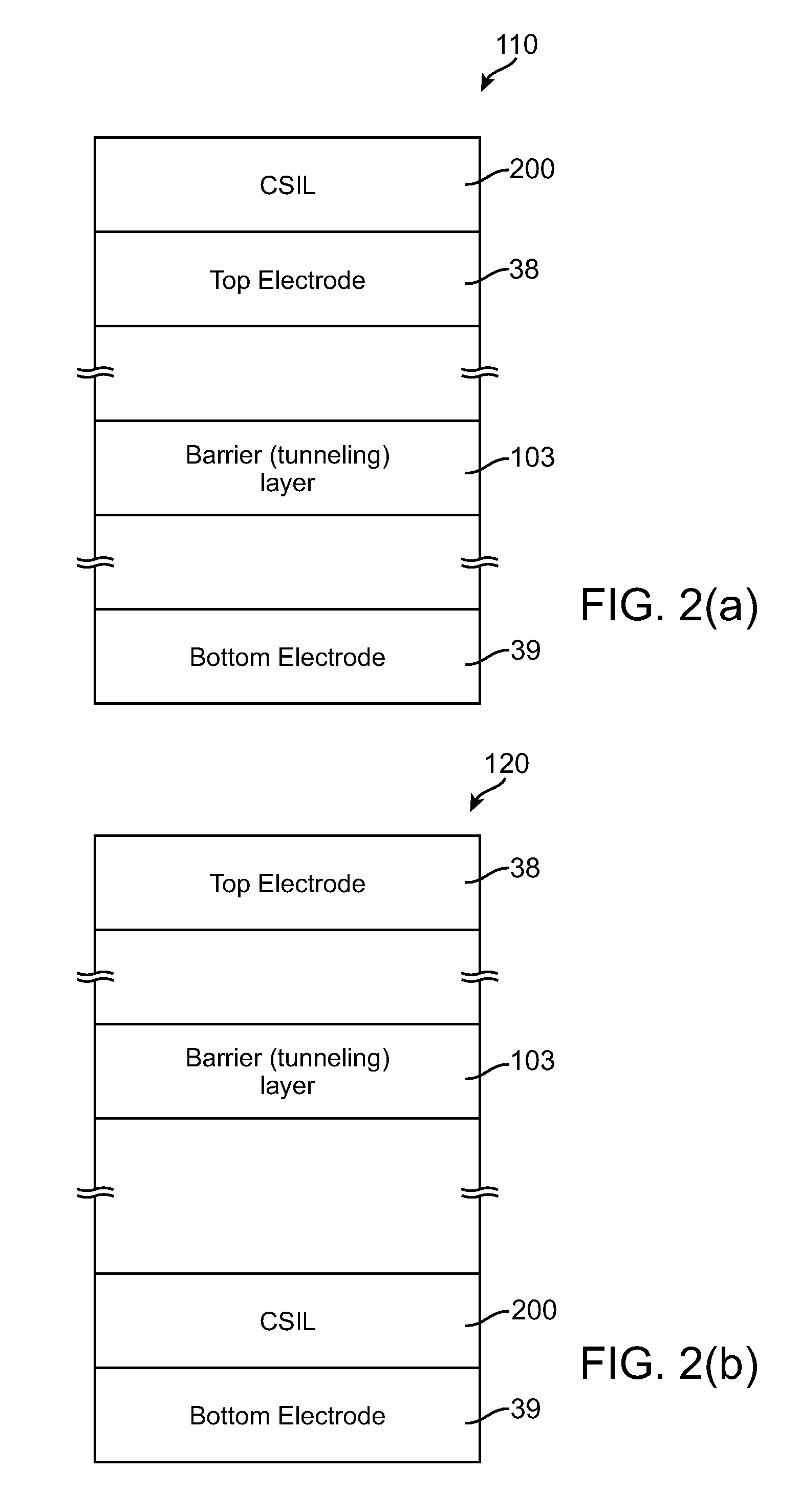
[0025]In the following description of the embodiments, reference is made to the accompanying drawings that form a part hereof, and in which is shown by way of illustration of the specific embodiments in which the invention may be practiced. It is to be understood that other embodiments may be utilized because structural changes may be made without departing from the scope of the present invention. It should be noted that the figures discussed herein are not drawn to scale and thicknesses of lines are not indicative of actual sizes.

[0026]The following are herein incorporated by reference as though set forth in full:

U.S. application Ser. No. 11 / 674,124, filed Feb. 12, 2007, titled “Non-Uniform Switching Based Non-Volatile Magnetic Based Memory” by Ranjan et alia,

U.S. application Ser. No. 11 / 678,515, Filed Feb. 23, 2007, titled “A high capacity low cost multi-state magnetic memory” by Ranjan et alia,

U.S. application Ser. No. 11 / 739,648 Filed Apr. 24, 2007, titled “Non-volatile magnetic...


PUM


Abstract

One embodiment of the present invention includes a non-volatile magnetic memory element including a fixed layer, a barrier layer formed on top of the fixed layer, and a free layer formed on top of the barrier layer, wherein the electrical resistivity of the barrier layer is reduced by placing said barrier layer under compressive stress. Compressive stress is induced by either using a compressive stress inducing layer, or by using inert gases at low pressure during the sputtering process as the barrier layer is deposited, or by introducing compressive stress inducing molecules into the molecular lattice of the barrier layer.

Description

CROSS REFERENCE TO RELATED APPLICATION[0001]This application is a continuation-in-part of U.S. application Ser. No. 11 / 674,124 filed on Feb. 12, 2007, entitled “Non-Uniform Switching Based Non-Volatile Magnetic Based Memory,” which claims priority to U.S. Provisional Application No. 60 / 853,115 filed on Oct. 20, 2006 entitled “Non-Uniform Switching Based Non-Volatile Magnetic Based Memory”; and is a further continuation-in-part of U.S. application Ser. No. 11 / 678,515 filed Feb. 23, 2007, entitled “A High Capacity Low Cost Multi-State Magnetic Memory,” which claims priority to U.S. Provisional Application No. 60 / 777,012 filed Feb. 25, 2006 entitled “A High Capacity Low Cost Multi-State Magnetic Memory”; and is a further continuation-in-part of U.S. application Ser. No. 11 / 739,648, filed Apr. 24, 2007 entitled “Non-Volatile Magnetic Memory with Low Switching Current and High Thermal Stability”; and is a further continuation-in-part of U.S. application Ser. No. 11 / 740,861, filed Apr. 26...

Claims


Application Information

Patent Timeline
IPC IPC(8): H01L29/82H01L21/00
CPCG11C11/16H01L43/12H01L43/08G11C11/161G11C11/1673G11C11/5607G11C11/1675H10N50/01H10N50/10
Inventor RANJAN, RAJIV YADAVKESHTBOD, PARVIZMALMHALL, ROGER KLAS
Owner AVALANCHE TECH
Why Eureka
Try Eureka