Multilayered Film-Nanowire Composite, Bifacial, and Tandem Solar Cells

a solar cell and composite technology, applied in the field of solar cells, can solve the problems of preventing the widespread use of such solar cell technology, unable to meet the needs of bifacial and bifacial fusion, and no one is efficient enough to significantly reduce the cost involved in the production and use of this technology, and achieve the effect of preventing shorting

Inactive Publication Date: 2008-07-17
GENERAL ELECTRIC CO
View PDF19 Cites 129 Cited by
  • Summary
  • Abstract
  • Description
  • Claims
  • Application Information

AI Technical Summary

Benefits of technology

[0015]Advantageously, the photoactive devices are multi-junction arrays that capture broad spectrum of light energy and, in some embodiments incorporate materials between elongated nanostructures to prevent shorting.

Problems solved by technology

Single and multi-junction p-n solar cells are used for this purpose, but none are efficient enough to significantly reduce the costs involved in the production and use of this technology.
Consequently, competition from conventional sources of electricity precludes the widespread use of such solar cell technology.
Abrupt band bending at a heterojunction due to a change in conductivity type and / or variations in band gap may lead to a high density of interface states that result in charge carrier recombination.
Defects introduced at the junction during fabrication may further act as sites for charge carrier recombination that degrade device performance.
While the ideal thermodynamic efficiency of a solar converter is ˜85%, there is a loss in efficiency due to the fact that sub-bandgap energy photons in the solar spectrum are not absorbed.
Additionally, recombination of photo-generated electrons and holes with trap states in the semiconductor crystal associated with point defects (interstitial impurities), metal clusters, line defects (dislocations), planar defects (stacking faults), and / or grain boundaries further reduces the efficiency.
Although this latter reduction in efficiency can be overcome by using other materials with appropriate properties (particularly long diffusion lengths of the photo-generated carriers), this still does not bring this technology to a cost parity with more conventional sources of electricity.
Because charge carriers can recombine at defect sites and are therefore lost as current carriers, defects typically adversely affect the operation or performance of electronic and / or optoelectronic devices such as solar cells.
The absorption capacity of the materials making up a PV device may also affect the efficiency of the cell.
Such arrays, however, were not configured for use in photovoltaic devices, nor was it suggested how such arrays might serve to increase the efficiency of solar cells.
However, such nanowires are not active photovoltaic (PV) elements; they merely serve in an anti-reflective capacity.

Method used


Image

  • Multilayered Film-Nanowire Composite, Bifacial, and Tandem Solar Cells
  • Multilayered Film-Nanowire Composite, Bifacial, and Tandem Solar Cells
  • Multilayered Film-Nanowire Composite, Bifacial, and Tandem Solar Cells

Examples


Embodiment Construction

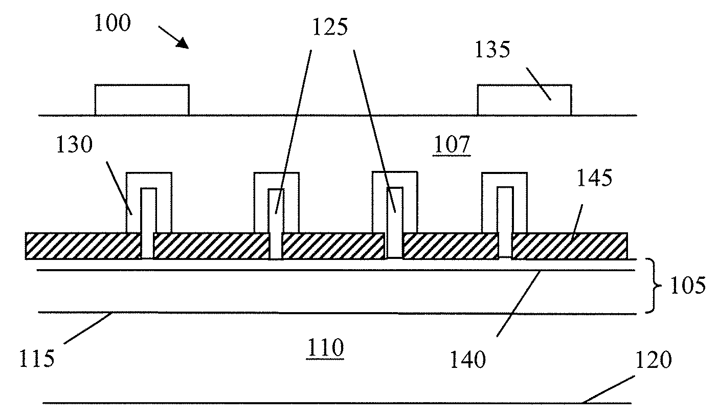
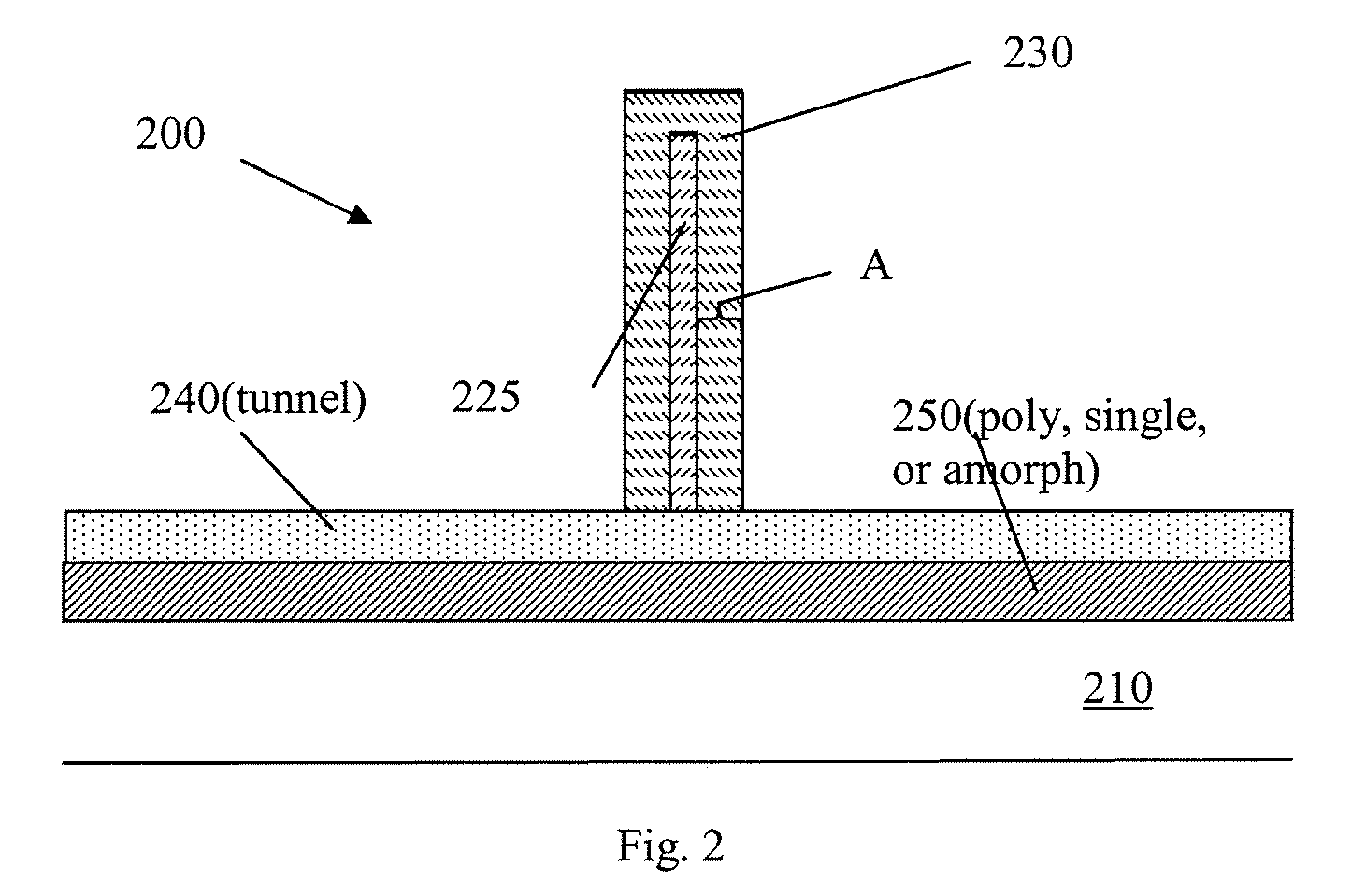
[0024]In some embodiments, a photovoltaic (PV) device may include, but is not limited to: (1) a multilayered film disposed on a substrate (2) elongated nanostructures, which may be disposed on the top layer of the multilayered film, and (3) at least one layer disposed over the elongated nanostructures. These layers disposed over the elongated nanostructures may be conformally disposed over the elongated nanostructures. The various layers of the multilayered film and the layers disposed about the elongated nanostructures may form portions of photoactive junctions, such as p-n and p-i-n junctions, for example. These photoactive junctions may be stacked with tunnel junctions separating each cell in the multi-junction array. Each cell in the multi-junction array may be arranged in series and may include p-n junctions, p-i-n junctions, and combinations thereof. In some embodiments, the elongated nanostructures may be part of a photoactive junction and be appropriately doped with p-dopant...


PUM


Abstract

A photovoltaic device includes a substrate having at least two surfaces and a multilayered film disposed on at least a portion of at least one surface of the substrate. Elongated nanostructures are disposed on the multilayered film. The device incorporates a top layer of the multilayered film contacting the elongated nanostructures that is a tunnel junction. The device has at least one layer deposited over the elongated nanostructures defining a portion of a photoactive junction. A solar panel includes at least one photovoltaic device. The solar panel isolates each such devices from its surrounding atmospheric environment and permits the generation of electrical power.

Description

RELATED APPLICATIONS[0001]This present application is related to commonly assigned co-pending application U.S. Ser. No. 11 / 599,722, filed Nov. 15, 2006, entitled “Graded Hybrid Amorphous Silicon Nanowire Solar Cells” and co-pending application U.S. Ser. No. 11 / 599,677, filed Nov. 15, 2006, entitled “Amorphous-Crystalline Tandem Nanostructured Solar Cells,” and to commonly assigned co-pending application U.S. Ser. No. ______, filed concurrently herewith, entitled “Nanowall Solar Cells and Optoelectronic Devices.”TECHNICAL FIELD[0002]The present invention relates generally to solar cells, and more specifically to such solar cells that may include elongated nanostructures disposed over a multilayered film.BACKGROUND INFORMATION[0003]Presently, silicon (Si) is the most commonly used material in the fabrication of solar cells, such solar cells being used for converting sunlight into electricity. Single and multi-junction p-n solar cells are used for this purpose, but none are efficient e...

Claims


Application Information

Patent Timeline
Patent Type & Authority Applications(United States)
IPC IPC(8): H01L31/042
CPCH01L31/035281H01L31/03529H01L31/0687H01L31/076Y02E10/544Y10S977/72H01L31/078Y10S977/948Y10S977/954Y10S977/712Y10S977/76Y02E10/548Y02P70/50
Inventor KOREVAAR, BASTIAAN ARIETSAKALAKOS, LOUCAS
Owner GENERAL ELECTRIC CO
Why Eureka
Try Eureka