Semiconductor device having a pseudo power supply wiring

a technology of power supply and circuit, which is applied in the direction of logic circuit coupling/interface arrangement, pulse technique, instruments, etc., can solve the problems of inadequacies of using the circuit shown in fig

Active Publication Date: 2008-07-17
MICRON TECH INC
View PDF6 Cites 4 Cited by
  • Summary
  • Abstract
  • Description
  • Claims
  • Application Information

AI Technical Summary

Benefits of technology

[0034]As described above, in the semiconductor device according to the present invention, the first and second gate circuits have the same configuration to each other. As a result, it becomes possible to retain a symmetric property of the complementary...

Problems solved by technology

Thus, there occurs a problem in that a sub-threshold current of a transistor in an off state increases.
Thus, when the enable signal E is the low level, it is not possible to render pseudo power supply wiring non-conducting the in the standby state, and as a result, there oc...

Method used


Image

  • Semiconductor device having a pseudo power supply wiring
  • Semiconductor device having a pseudo power supply wiring
  • Semiconductor device having a pseudo power supply wiring

Examples


first embodiment

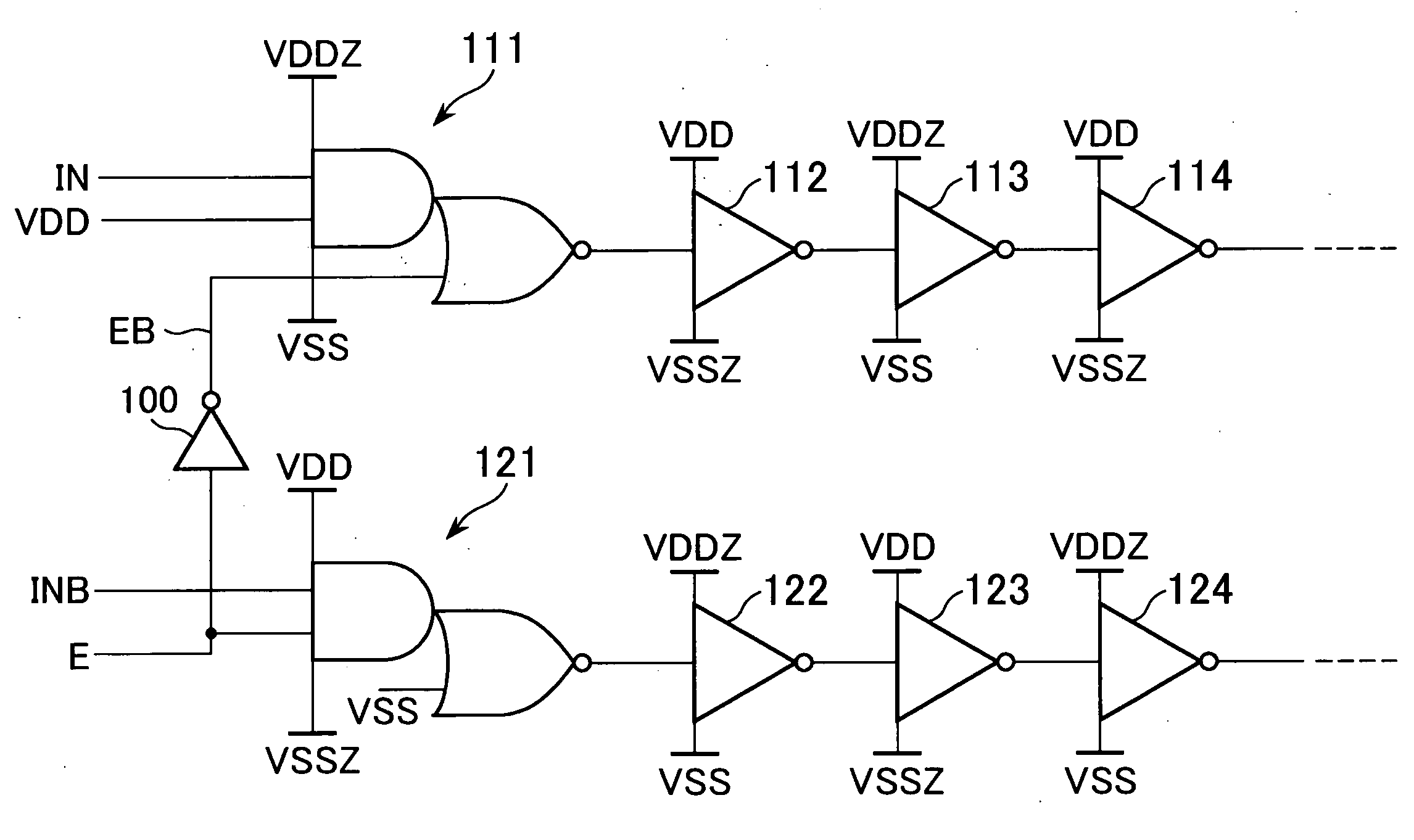
[0056]FIG. 1 is a circuit diagram of a semiconductor device according to a preferred first embodiment of the present invention.

[0057]As shown in FIG. 1, the semiconductor device according to the present embodiment includes a first AND-NOR composite gate 111 and a second AND-NOR composite gate 121 to which complementary input signals IN and INB are supplied, respectively. At later stages of the first and second AND-NOR composite gates 111 and 121, various gate circuits are dependently connected. In the present embodiment, as an example, inverters 112 to 114, . . . and 122 to 124, . . . are dependently connected, respectively.

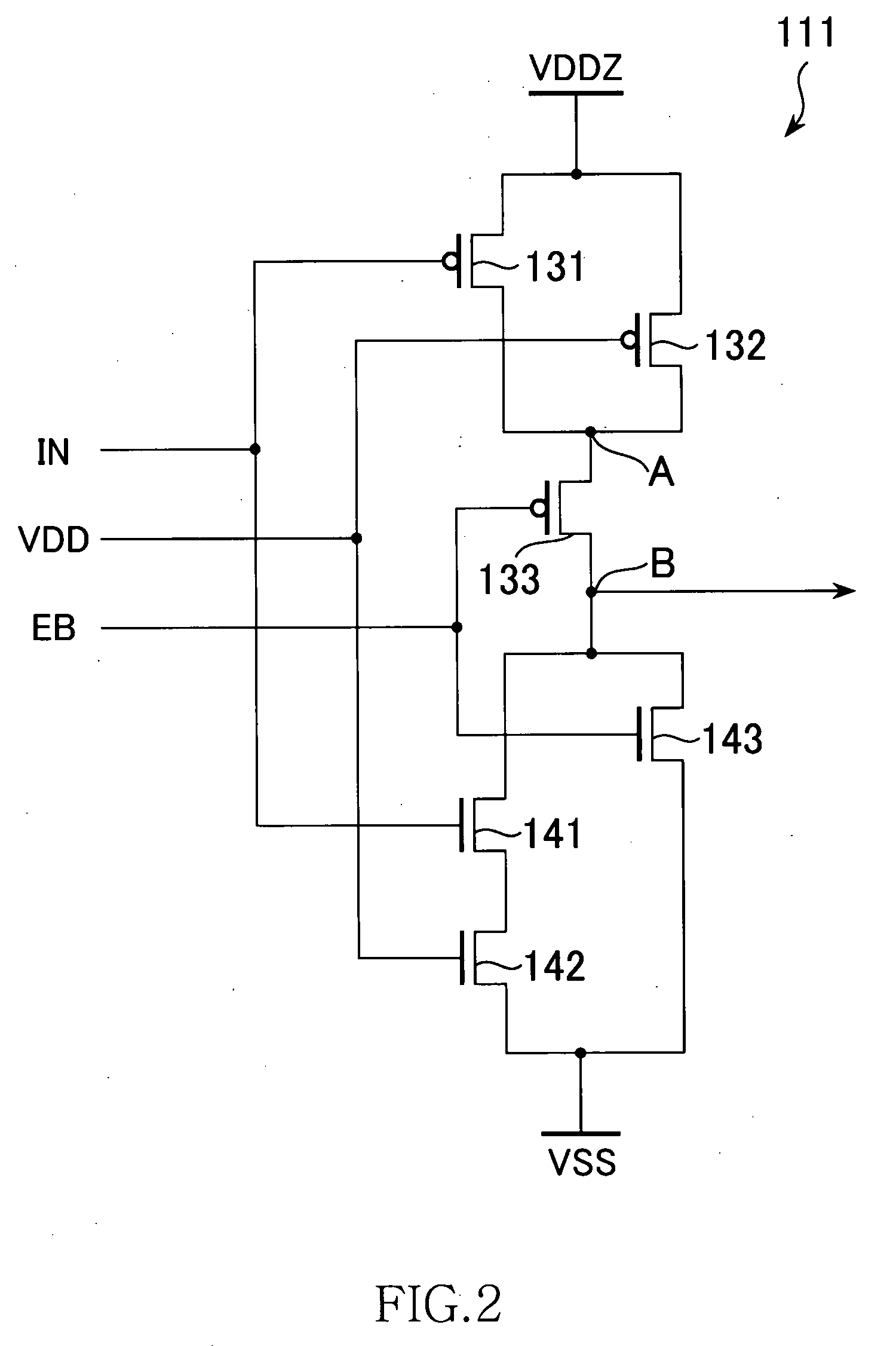
[0058]The first AND-NOR composite gate 111 is a 3-input composite gate circuit, and is configured logically of a 2-input AND-based logical unit (AND unit), and an OR-based logical unit (NOR unit) that receives output of the AND-based logical unit and third input. The AND-based logical unit (AND unit) is supplied with an input signal IN and an electric potential (...

second embodiment

[0073]A preferred second embodiment of the present invention is explained next.

[0074]FIG. 4 is a circuit diagram of a semiconductor device according to the second embodiment of the present invention.

[0075]As shown in FIG. 4, in the semiconductor device of the present embodiment, the first and second AND-NOR composite gates 111 and 121 shown in FIG. 1 are replaced by first and second OR-NAND composite gates 211 and 221, respectively.

[0076]The first OR-NAND composite gate 211 is a 3-input composite gate circuit, and configured logically of a 2-input OR-based logical unit (OR unit) and an AND-based logical unit (NAND unit) that receives output of the OR-based logical unit and third input. The OR-based logical unit (OR unit) is supplied with the input signal IN and the signal EB obtained by inverting the enable signal E by an inverter 200, and the AND-based logical unit (NAND unit) is supplied with the electric potential of the main power supply wiring VDD. As shown in FIG. 1, power sup...

third embodiment

[0084]A preferred third embodiment of the present invention is explained next.

[0085]FIG. 7 is a circuit diagram of a semiconductor device according to the third embodiment of the present invention.

[0086]As shown in FIG. 7, in the semiconductor device according to the present embodiment, the first and second AND-NOR composite gates 111 and 121 shown in FIG. 1 are replaced by NAND circuits 311 and 321, and the inverters 112 and 122 are replaced by NAND circuits 312 and 322, respectively.

[0087]The NAND circuits 311, 312, 321, and 322 are each 2-input NAND circuits. The NAND circuit 311 is supplied with the input signal IN and the electric potential of the main power supply wiring VDD, and the NAND circuit 312 is supplied with output of the NAND circuit 311 and the enable signal E. On the other hand, the NAND circuit 321 is supplied with the input signal INB and the enable signal E, and the NAND circuit 322 is supplied with output of the NAND circuit 321 and the electric potential of th...


PUM


Abstract

A semiconductor device including an AND-NOR composite gate of which AND unit is supplied with input signals IN and VDD and NOR unit is supplied with an inverted signal EB of an enable signal E, and an AND-NOR composite gate of which AND unit is supplied with an input signal INB and an enable signal E and NOR unit is supplied with VSS. These gates are inserted into a path to which the input signals IN and INB are supplied. Thereby, a symmetric property of a complimentary signal can be retained. Further, outputs of the AND-NOR composite gates are fixed irrespective of a logical level of the enable signal E. Thus, a sub-threshold current also is inhibited.

Description

TECHNICAL FIELD[0001]The present invention relates to a semiconductor device having a pseudo power supply wiring for reducing power consumption in a standby state. More specifically, the present invention relates to a semiconductor device including a path that transmits a complementary input signal.BACKGROUND OF THE INVENTION[0002]In recent years, an operating voltage of a semiconductor device is gradually decreasing for the purposes of reducing consumption power, and at present, a very low voltage of as low as 1 bolt is sometimes used. When the operating voltage decreases, a threshold voltage of a transistor needs to be decreased. Thus, there occurs a problem in that a sub-threshold current of a transistor in an off state increases. To solve such a problem, a method of dividing a power supply wiring into a main power supply wiring and a pseudo power supply wiring is proposed in Japanese Patent Application Laid-open Nos. 2000-13215 and 2000-48568.[0003]FIG. 15 is a circuit diagram o...

Claims


Application Information

Patent Timeline
IPC IPC(8): H03K19/0175
CPCH03K19/018521H03K19/0013
Inventor HAYASHI, JUNICHINODA, HIROMASA
Owner MICRON TECH INC
Why Eureka
Try Eureka