Semiconductor integrated circuit and data processing system

Inactive Publication Date: 2008-07-24
RENESAS ELECTRONICS CORP
View PDF13 Cites 7 Cited by
  • Summary
  • Abstract
  • Description
  • Claims
  • Application Information

AI Technical Summary

Benefits of technology

[0012]Namely, this invention can achieve increase in the data transmission ra

Problems solved by technology

In such a multichip configuration, these multiple LSIs individually have a data processing memory, thus increasing the number of components and the cost.
An increase in the number of components also leads to an increase in the mounting area of a set, resulting in also an obstacle for achieving miniaturization and high density mounting of the set.
By the same token, since the signals are wire-connec

Method used


Image

  • Semiconductor integrated circuit and data processing system
  • Semiconductor integrated circuit and data processing system
  • Semiconductor integrated circuit and data processing system

Examples


Example

[0021]First, an overview concerning a representative embodiment of the invention disclosed in the present application will be described. Reference numerals in the accompanying drawings that are referred to with a parenthesis in the overview description concerning the representative embodiment just exemplify the one contained in the concept of a constituent element with the parenthesized reference numeral.

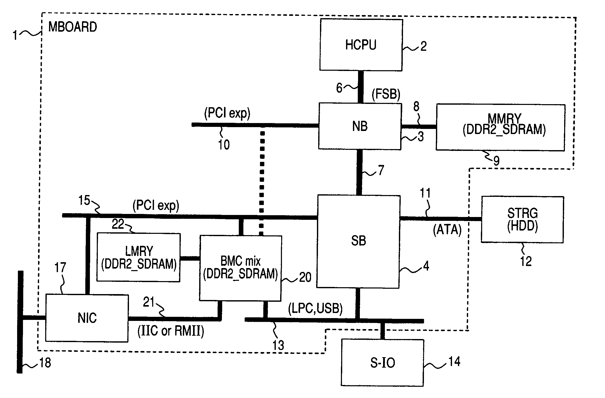
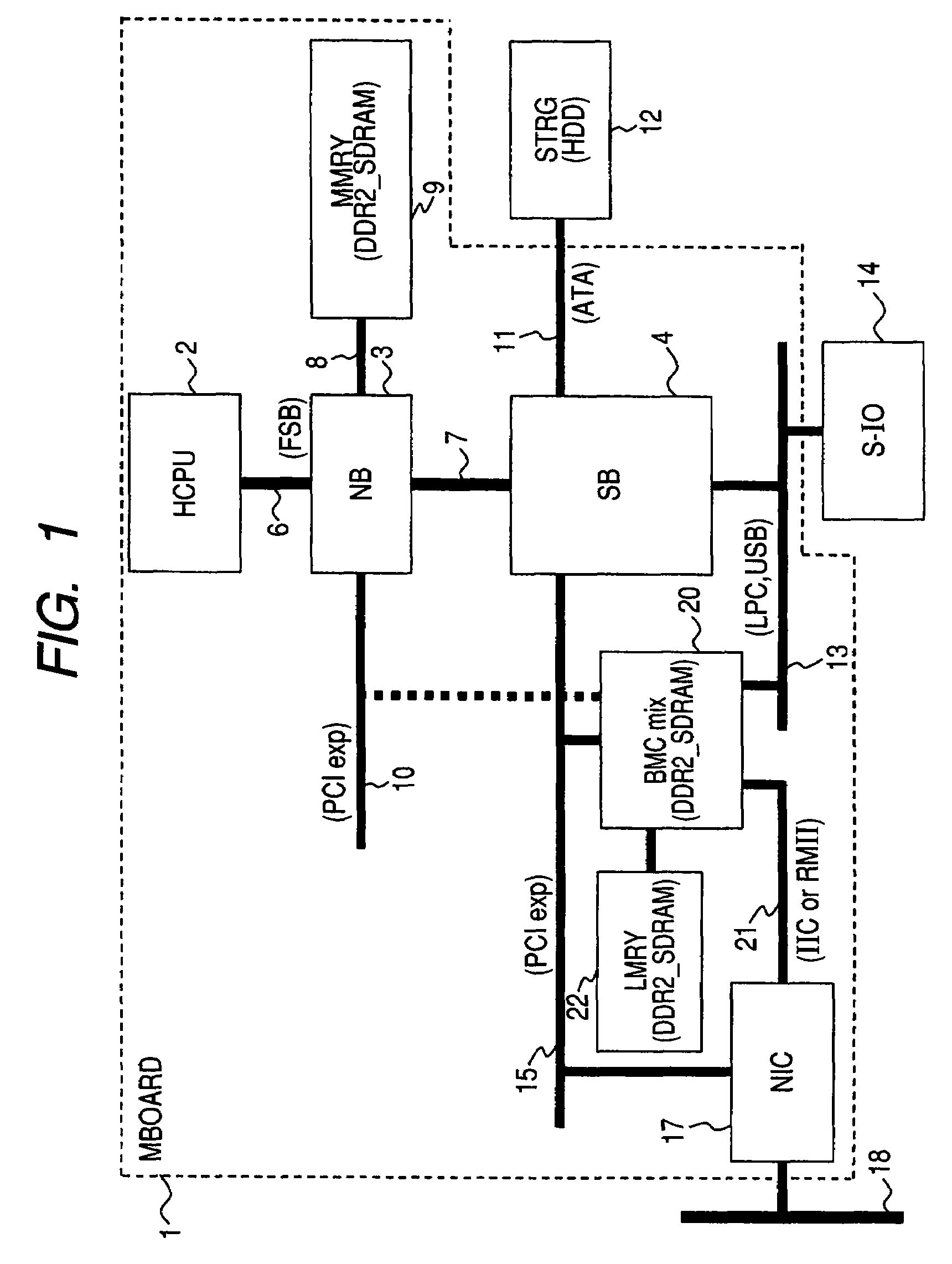
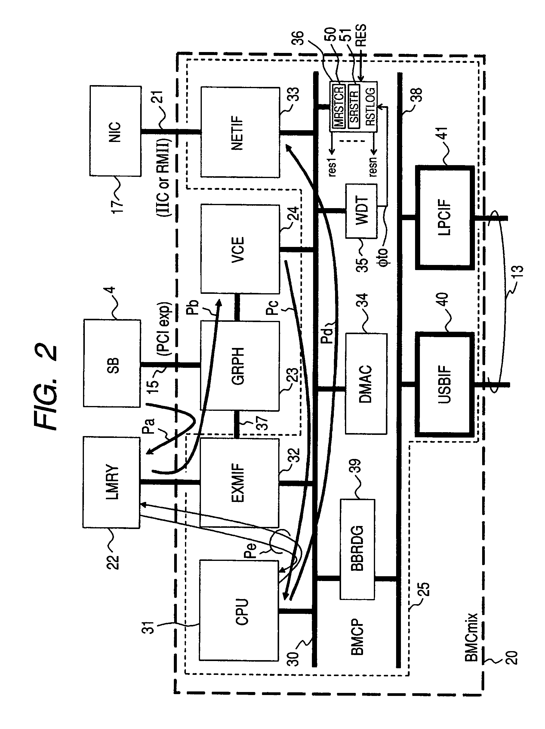
[0022][1] A semiconductor integrated circuit (20) concerning a representative embodiment of the present invention comprises in one semiconductor substrate: an image processing unit (23) that performs image processing in response to an input from an external bus (15); a compression unit (24) coupled to the image processing unit and capable of compressing an image data; and an interface unit (25) that may be utilized for server management. The interface unit includes a central processing unit (31), an external memory interface circuit (32), and a network interface circuit (33) that ar...


PUM


Abstract

To contribute to increase data transmission rate for server management without increasing load during normal operation.
A semiconductor integrated circuit includes: a central processing unit; an external memory interface circuit; a network interface circuit; an image processing unit; and a data compression unit. The image processing unit performs image processing in response to an input from an external bus, the image processing unit is coupled to an external memory interface circuit through a dedicated internal bus, and the image processing unit stores an image data into an external memory via the dedicated internal bus. The compression unit is coupled to the image processing unit and is capable of compressing the image data supplied from the image processing unit. Since the dedicated internal bus, through which the image processing unit receives image information and stores the same into the external memory, is separated from the common internal bus, the data for image processing by the image processing unit that responds to an instruction from the outside will not conflict with the data for data processing by an instruction from the network interface circuit on the common internal bus.

Description

CROSS-REFERENCE TO RELATED APPLICATION[0001]The disclosure of Japanese Patent Application No. 2007-11137 filed on Jan. 22, 2007 including the specification, drawings and abstract is incorporated herein by reference in its entirety.BACKGROUND OF THE INVENTION[0002]The present invention relates to semiconductor integrated circuits that may be utilized for remote management of a server, and furthermore to semiconductor integrated circuits for achieving an interface function compliant with IPMI (Intelligent Platform Management Interface) or the like, and relates to techniques effectively applied to a data processing system, such as a server with a remote management function, for example.[0003]A general motherboard for a computer includes: a main CPU; a north bridge such as a memory controller hub; a south bridge such as an I / O controller hub; a graphics controller; a network interface controller; a peripheral input output circuit (a keyboard, a mouse, an FDD, a CD-ROM, a serial port, a ...

Claims


Application Information

Patent Timeline
IPC IPC(8): G06F13/38
CPCG06F11/0793G06F11/0748
Inventor ONDA, MICHIO
Owner RENESAS ELECTRONICS CORP
Why Eureka
Try Eureka