Photovoltaic device and process for producing same

a photovoltaic device and photovoltaic technology, applied in the direction of solid-state devices, final product manufacturing, basic electric elements, etc., can solve the problems of marked decrease in electric power generation efficiency, unsuitable structure for electric cells, and dramatic deterioration of open-circuit voltage and fill factor, and achieve high photovoltaic conversion efficiency and high level of productivity

Inactive Publication Date: 2008-08-21
MITSUBISHI HEAVY IND LTD
View PDF11 Cites 103 Cited by
  • Summary
  • Abstract
  • Description
  • Claims
  • Application Information

AI Technical Summary

Benefits of technology

[0017]The present invention has been developed in light of the above circumstances, and has an object of providing a photovoltaic device and a process for producing such a device that combine a high photovoltaic conversion efficiency with a high level of productivity.
[0018]Furthermore, another object of the present invention is to provide a photovoltaic device that uses a transparent electrode-bearing substrate in which the haze ratio has been increased by using a mixture of coarse and fine roughness, wherein a high photovoltaic conversion efficiency can be achieved with favorable suppression of any reductions in the open-circuit voltage and the fill factor, and also to provided a process for producing such a photovoltaic device.

Problems solved by technology

Conventionally, it has generally been thought that if the haze ratio of the substrate incorporating the first transparent electrode is increased, then although the light containment effect is improved by scattering of the incident light, which increases the electric power generation current, the open-circuit voltage and fill factor deteriorate dramatically due to the effects of the coarse roughness on the surface of the substrate incorporating the first transparent electrode, meaning the resulting structure is unsuitable as an electric cell.
However, if the film thickness of the bottom cell within a tandem solar cell is reduced to less than 2 μm, then a dramatic reduction occurs in the electric power generation current, causing a marked decrease in the electric power generation efficiency.
The technique disclosed within the above patent citation 1 pays no particular consideration to the electric power generation efficiency of the photovoltaic layers comprising crystalline silicon-based semiconductors with different light absorption wavelength properties, and furthermore, makes no investigation of productivity improvements for solar cells.

Method used


Image

  • Photovoltaic device and process for producing same
  • Photovoltaic device and process for producing same
  • Photovoltaic device and process for producing same

Examples


first embodiment

[0091]A first embodiment of the present invention is described below with reference to the drawings.

[0092]First is a description of the structure of a photovoltaic device produced using a process for producing a photovoltaic device according to this embodiment.

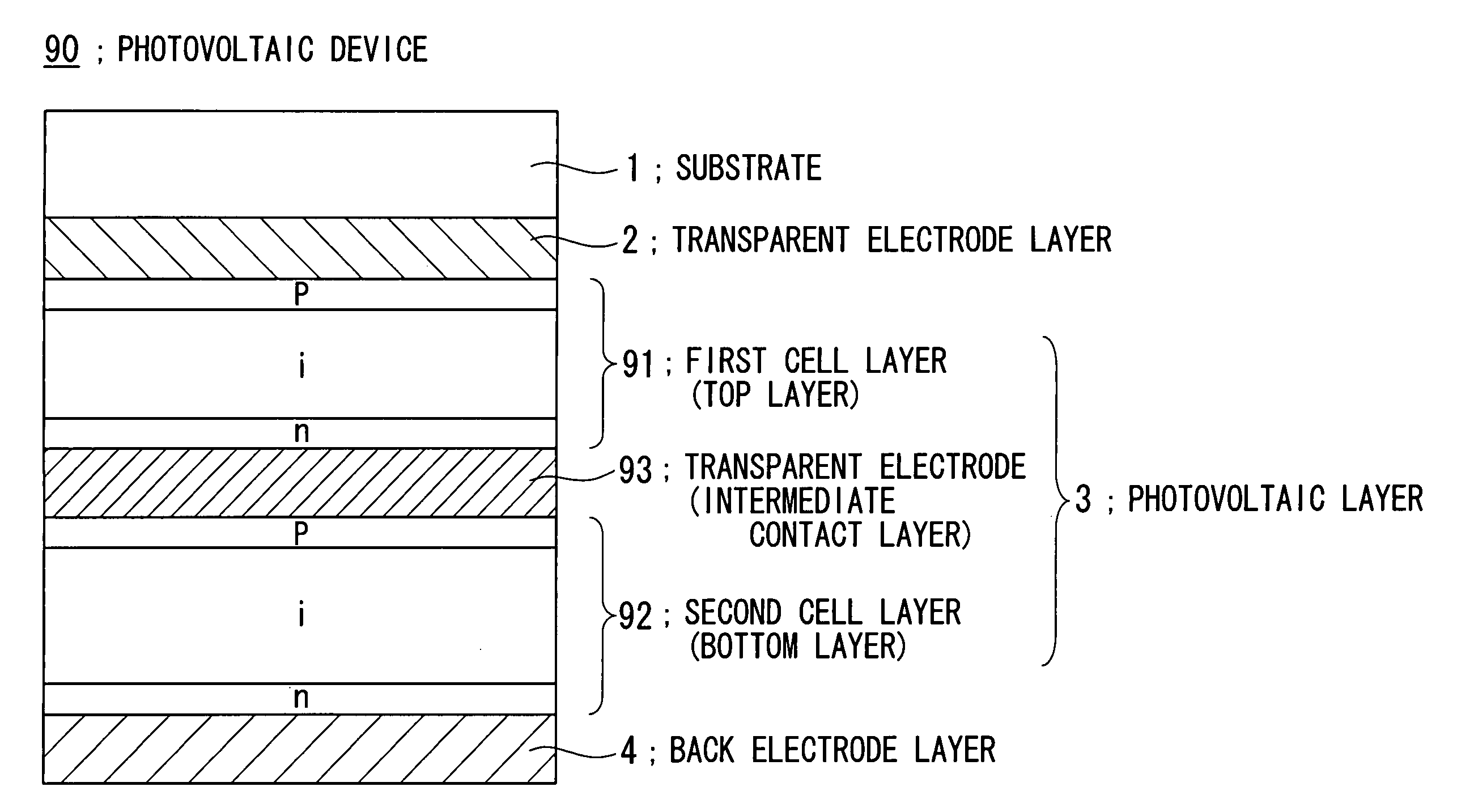
[0093]FIG. 1 is a schematic view showing the structure of a photovoltaic device according to this embodiment. The photovoltaic device 90 is a silicon-based solar cell, and comprises a substrate 1, a transparent electrode layer 2, a solar cell photovoltaic layer 3 comprising a first cell layer (a top layer) 91 and a second cell layer (a bottom layer 92, and a back electrode layer 4. In this embodiment, the first cell layer 91 is a photovoltaic layer comprising mainly amorphous silicon-based semiconductors, and the second cell layer is a photovoltaic layer comprising mainly crystalline silicon-based semiconductors. The second cell layer 92 has a film thickness of not less than 1.2 μm and not more than 2.0 μm, and the Raman ratio...

example 1

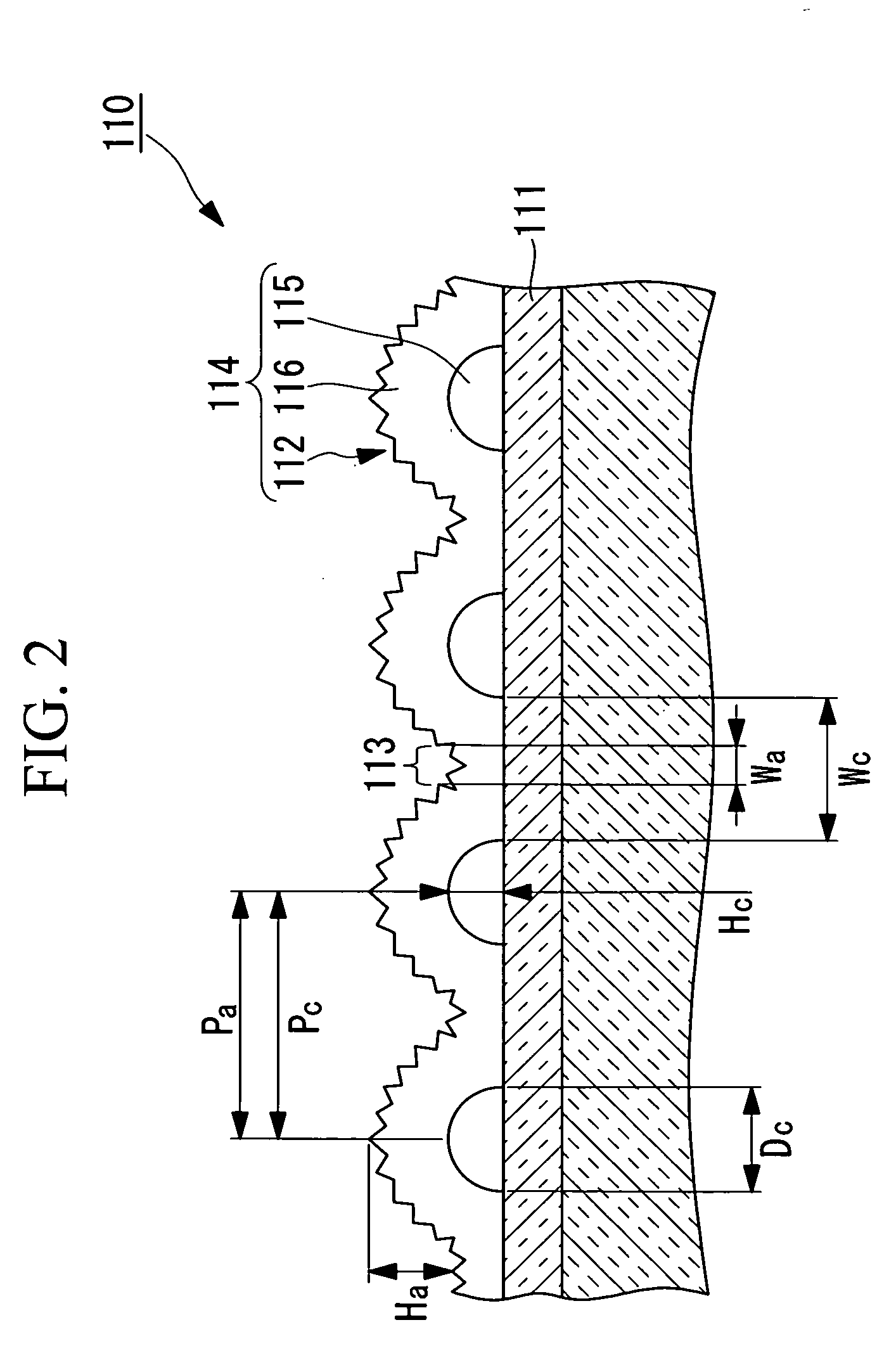
[0186]A tandem solar cell was produced in accordance with the embodiment of the present invention described above. A substrate with a double textured structure, prepared by depositing layers of SnO2 containing discontinuous small ridges and a plurality of micro-protrusions, was used as the transparent electrode-bearing substrate (height of ridges: 500 nm, density of ridges: 30 per 10 μm square). The film thickness values for the top cell i-layer and the bottom cell i-layer in this example were as shown in Table 1, and an intermediate contact layer was not formed.

[0187]The cell performance of the obtained solar cell is shown in Table 2. The initial value for the electric power generation efficiency for the solar cell of this example, in which the film thickness of the bottom cell i-layer was set to 2 μm relative to a film thickness for the top cell i-layer of 300 nm, was able to be increased to 13.3%. This is an effect of having been able to considerably increase the electrical curre...

example 2

[0190]With the exceptions of forming the top cell i-layer and the bottom cell i-layer with the film thickness values shown in Table 1, a tandem solar cell of the example 2(1) was produced using the same method as the example 1.

[0191]The cell performance of the obtained solar cell is shown in Table 2. The initial value for the electric power generation efficiency for the solar cell of this example, in which the film thickness of the bottom cell i-layer was set to 1.5 μm relative to a film thickness for the top cell i-layer of 300 nm, was 12.8%, indicating that relative to the comparative example 1, an improvement in efficiency and a reduction in the film thickness of the bottom cell by 25% were able to be achieved simultaneously. By using the transparent electrode-bearing substrate according to this embodiment of the present invention, the same effect as that described for the example 1 enables a high electric power generation current to be achieved even when the thickness of the bot...


PUM


Abstract

A photovoltaic device and a process for producing the photovoltaic device that combine a high photovoltaic conversion efficiency with a high level of productivity. The photovoltaic device includes at least a transparent electrode-bearing substrate, prepared by providing a transparent electrode layer on a transparent, electrically insulating substrate, and a photovoltaic layer containing mainly crystalline silicon-based semiconductors and a back electrode layer formed sequentially on the transparent electrode layer of the transparent electrode-bearing substrate, wherein the surface of the transparent electrode layer of the transparent electrode-bearing substrate has a shape that contains a mixture of coarse and fine roughness, and exhibits a spectral haze ratio of 20% or greater for wavelengths of from 550 nm to 800 nm, and the photovoltaic layer containing mainly crystalline silicon-based semiconductors has a film thickness of from 1.2 μm to 2 μm, and a Raman ratio of from 3.0 to 8.0.

Description

CROSS-REFERENCE TO RELATED APPLICATIONS[0001]This is a continuation of International Application PCT / JP2007 / 065386, with an international filing date of Aug. 6, 2007.BACKGROUND OF THE INVENTION[0002]1. Field of the Invention[0003]The present invention relates to a photovoltaic device and a process for producing the same, and relates particularly to a thin film silicon stacked solar cell that uses silicon as the electric power generation layer.[0004]2. Description of Related Art[0005]The use of silicon-based thin-film photovoltaic devices as photovoltaic devices such as solar cells is already known. These photovoltaic devices generally comprise a first transparent electrode, a silicon-based semiconductor layer (a photovoltaic layer), a second transparent electrode, and a back electrode deposited sequentially on top of a substrate. The semiconductor layer has a pin junction formed by p-type, i-type, and n-type semiconductor materials. In those cases where the photovoltaic device is a ...

Claims


Application Information

Patent Timeline
Patent Type & Authority Applications(United States)
IPC IPC(8): H01L31/028H01L31/076H01L31/077
CPCY02E10/546Y02E10/548H01L31/0236H01L31/076H01L31/056H01L31/182H01L31/1884Y02E10/52H01L31/077Y02E10/547Y02P70/50H01L31/04H01L27/14
Inventor NAKANO, YOUJITAKEUCHI, YOSHIAKIYAMAGUCHI, KENGOYAMAUCHI, YASUHIRO
Owner MITSUBISHI HEAVY IND LTD
Why Eureka
Try Eureka