Microfluidic Device for Patterned Surface Modification
- Summary
- Abstract
- Description
- Claims
- Application Information
AI Technical Summary
Benefits of technology
Problems solved by technology
Method used
Image

Examples
examples
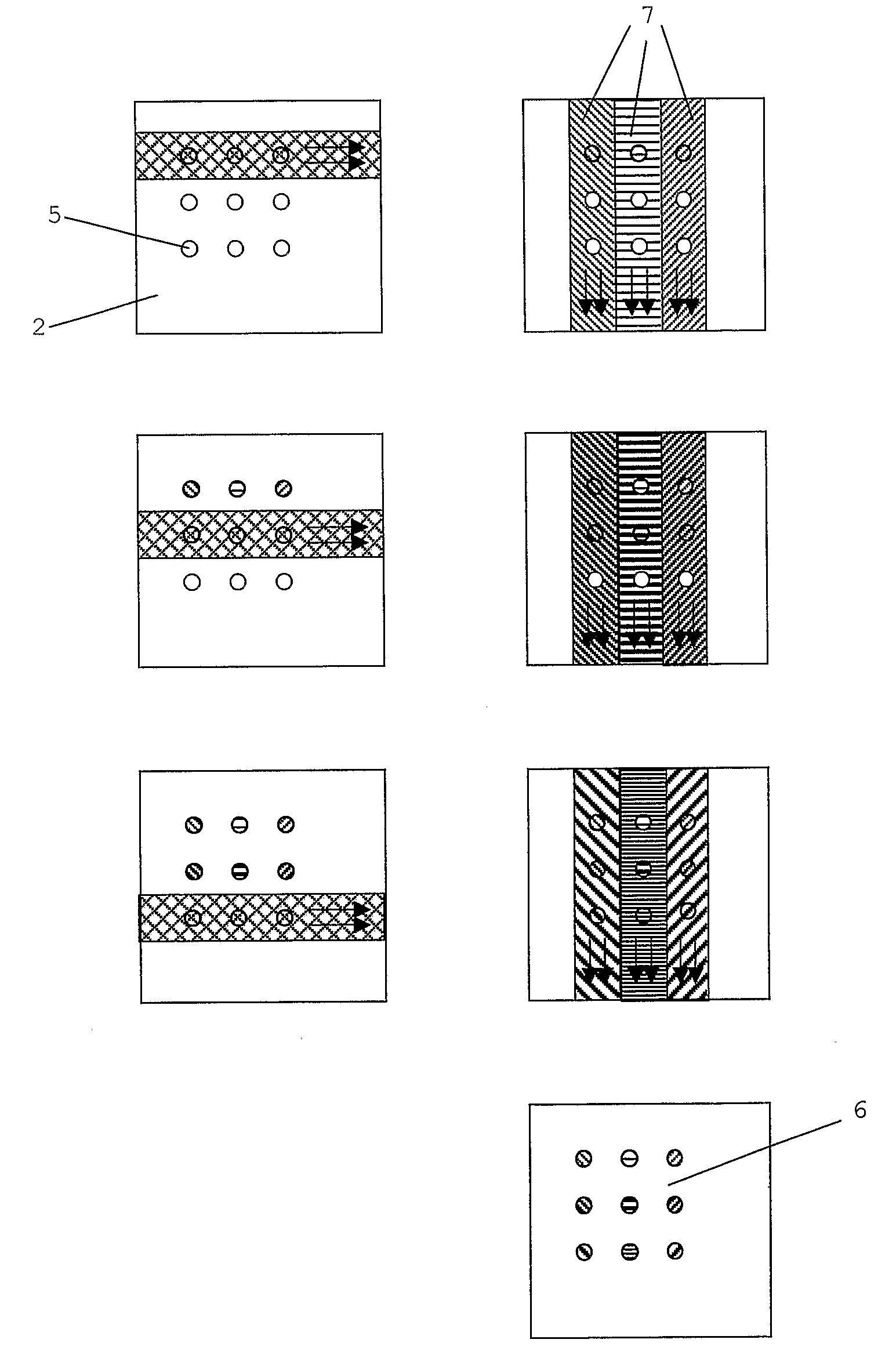
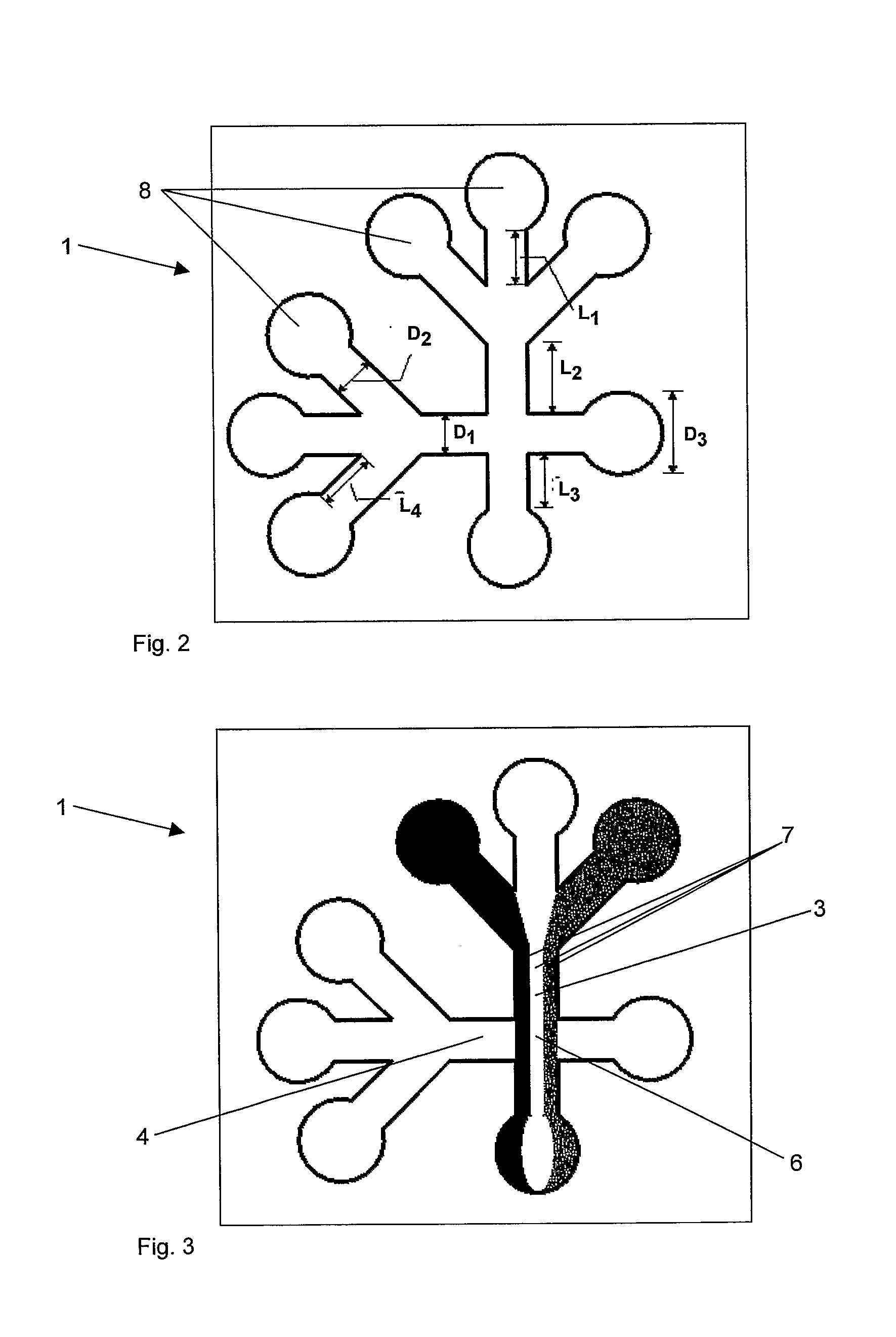
[0092]1. Production of the Flow Cell
[0093]1.1. Mould Production
[0094]For the production of the mould photolithographic technique was used. In this step a 4-inch silicon wafer from Wafernet GmbH, was cleaned and dried for 10 min in a plasma cleaner (300E from TePla). On this dry wafer 3 ml of photoresist (SU-8 50, MicroChem Company) was homogeneously applied by spincoating (max. speed: 1500 rpm, spincoater: RC 5 GYRSET from Karl Süss). Then the prebake was performed. Therefor the wafer was placed on a 50° C. warm hot plate for 5 min. The hot plate was then heated up to 100° C. and held at this temperature for 60 min. In the next step the wafer and the photomask (foil showing the design of the flow cell, 64′000 dpi, from jdphoto glued to a glass plate) were installed in a mask aligner (MA6 / BA6 from Karl Süss), where the photoresist was exposed to UV light through the mask for 44.4 sec to apply 400 J / cm 2. This exposure to UV light started a crosslinking reaction in the photoresist, w...
PUM
| Property | Measurement | Unit |
|---|---|---|
| Width | aaaaa | aaaaa |
| Width | aaaaa | aaaaa |
| Pressure | aaaaa | aaaaa |
Abstract
Description
Claims
Application Information
 - Generate Ideas
- Intellectual Property
- Life Sciences
- Materials
- Tech Scout
- Unparalleled Data Quality
- Higher Quality Content
- 60% Fewer Hallucinations
Browse by: Latest US Patents, China's latest patents, Technical Efficacy Thesaurus, Application Domain, Technology Topic, Popular Technical Reports.
© 2025 PatSnap. All rights reserved.Legal|Privacy policy|Modern Slavery Act Transparency Statement|Sitemap|About US| Contact US: help@patsnap.com