Multi-beam deflector array device for maskless particle-beam processing

Active Publication Date: 2008-08-28
INSTITUT FUER MIKROELEKTRONIK STUTTGART +1
View PDF13 Cites 50 Cited by
  • Summary
  • Abstract
  • Description
  • Claims
  • Application Information

AI Technical Summary

Benefits of technology

[0024]By configuring the substrate material of the DAP to act as ground electrode to the deflecting electrode, the production of individual ground electrodes providing ground potential is dispensable and the fabrication process of said device can be simplified. For this variant it is useful to provide a buried insulating layer between the deflecting electrodes and the substrate material, as for example SiO2 in a silicon-on-insulator (SOI) wafer.
[0025]In another variant of the inven

Problems solved by technology

There are several problematic issues in the use of pattern definition devices as described in prior art.
In particular the forming of the electrodes employing perpendicular growth is a rather complex process.
Additionally such electrodes are very sensitive to deformation and stress.
Moreover, electrodes that have a substantial height over the blanking plate impose a limitation of the electric field strength tolerable in the vicinity of the blanking plate (this is due to stray

Method used


Image

  • Multi-beam deflector array device for maskless particle-beam processing
  • Multi-beam deflector array device for maskless particle-beam processing
  • Multi-beam deflector array device for maskless particle-beam processing

Examples


Example

[0059]The preferred embodiments of the invention discussed in the following are related to a PML2-type particle-beam exposure apparatus with a pattern definition system as disclosed in the U.S. Pat. No. 6,768,125 (=GB 2,389,454 A) of the applicant / assignee, and with a large-reduction projecting system. In the following, first the technical background of the apparatus is discussed as far as relevant to the invention, and then embodiments of the invention are discussed in detail. It should be appreciated that the invention is neither restricted to the following embodiments nor to a pattern definition system, which merely represents one of the possible implementations of the invention.

PML2

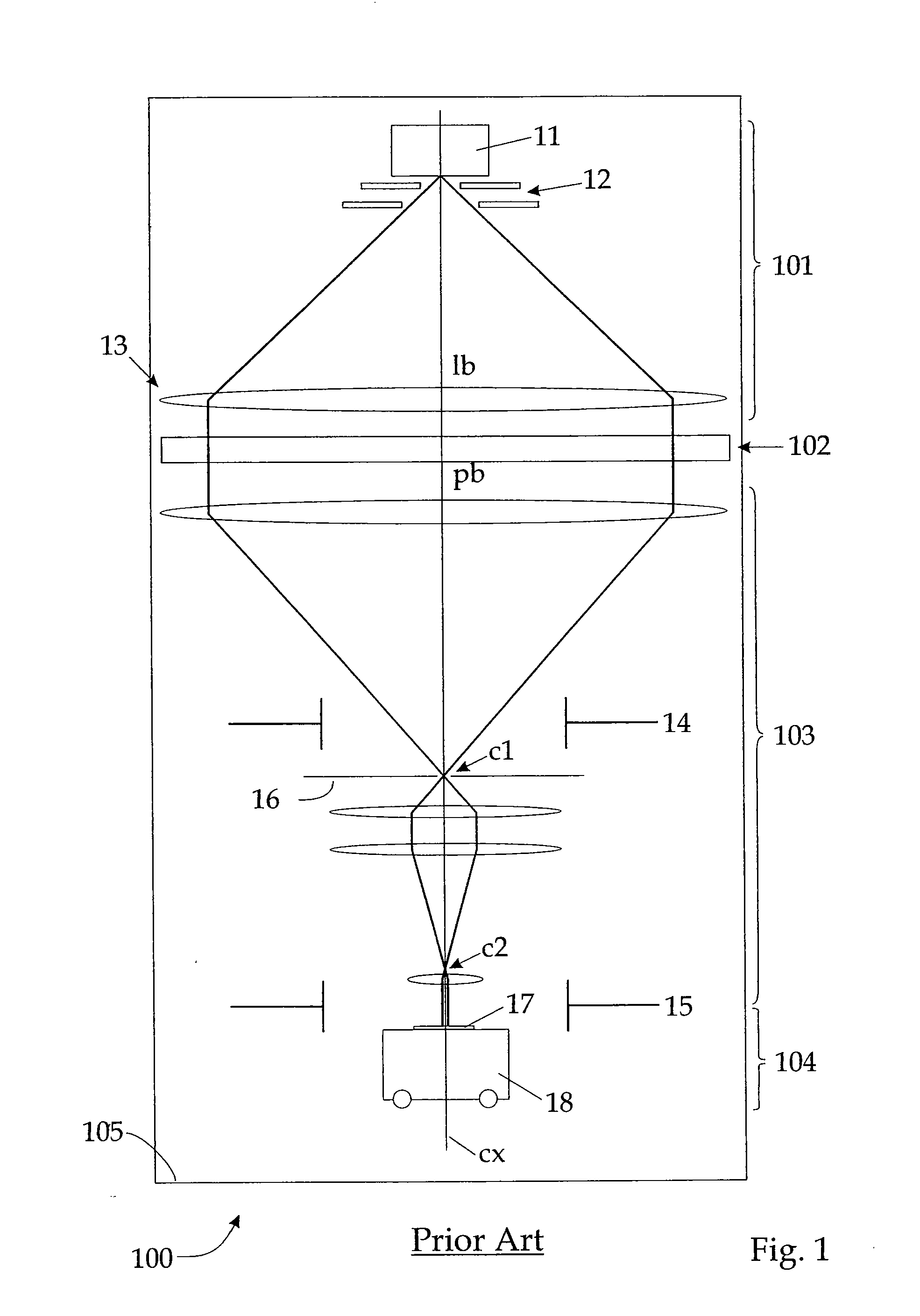
[0060]FIG. 1 shows an overview of a lithographic apparatus. For the sake of clarity, the components are not shown to size. The main components of the lithography apparatus 100 are—corresponding to the direction of the lithography beam lb, pb which runs vertically downward in FIG. 1—an illumination sys...


PUM


Abstract

The invention relates to a multi-beam deflector array device for use in a particle-beam exposure apparatus employing a beam of charged particles, the multi-beam deflector array device having a plate-like shape with a membrane region, the membrane region including a first side facing towards the incoming beam of particles, an array of apertures, each aperture allowing passage of a corresponding beamlet formed out of the beam of particles, a plurality of depressions, each depression being associated with at least one aperture, and an array of electrodes, each aperture being associated with at least one electrode and each electrode being located in a depression, the electrodes being configured to realize a non-deflecting state, wherein the particles that pass through the apertures are allowed to travel along a desired path, and a deflecting state, wherein the particles are deflected off the desired path.

Description

FIELD OF THE INVENTION[0001]The present invention relates to a multi-beam deflector array device for a maskless particle-beam exposure apparatus for forming a pattern on a surface of a substrate by means of a multitude of beams of energetic charged particles. More in detail, the invention relates to a multi-beam deflector array device as part of a pattern definition means for use in a maskless particle-beam exposure apparatus.[0002]Furthermore, the invention relates to a method for producing said multi-beam deflector array device.BACKGROUND[0003]In a particle-beam exposure apparatus, a particle beam is generated by an illumination system and illuminates a pattern definition means having an array of apertures which define a beam pattern to be projected on a target surface. One important application of a particle-beam exposure apparatus of this kind is in the field of nano-scale patterning, by direct ion beam material modification or by electron or ion beam induced etching and / or depo...

Claims


Application Information

Patent Timeline
IPC IPC(8): H01J3/14H01L21/20
CPCB82Y10/00B82Y40/00G03F1/20H01J2237/0437H01J37/045H01J37/3174H01J37/3177G03F7/2059
Inventor PLATZGUMMER, ELMARLOSCHNER, HANSKVASNICA, SAMUELSPRINGER, REINHARDIRMSCHER, MATHIASLETZKUS, FLORIANBUTSCHKE, JORG
Owner INSTITUT FUER MIKROELEKTRONIK STUTTGART
Why Eureka
Try Eureka