Assembly of two parts of an integrated electronic circuit

a technology of integrated electronic circuit and assembly process, which is applied in the direction of electrically conductive connections, electrical apparatus construction details, and solvent media, etc., can solve the problems of long and difficult wire bonding, limited number of wire bonding connections, and limited number of electrical connections which can be implemented in this manner, so as to achieve more reliability in connection and reduce the robustness of the process of establishing a reliable electrical connection

Active Publication Date: 2008-08-28
STMICROELECTRONICS (CROLLES 2) SAS
View PDF35 Cites 69 Cited by
  • Summary
  • Abstract
  • Description
  • Claims
  • Application Information

AI Technical Summary

Benefits of technology

[0027]Alternatively, the initial materials of the two connection portions may be selected such that the conductive alloy which is formed in step / 2 / at least partially fills the recess by a volumetric expansion of the alloy relative to the initial materials. The connection between the two connection portions then results from this volumetric expansion, without requiring significant diffusion of one of the initial materials.
[0028]In one embodiment, at least one of the two connection portions may initially contain quantities of all the materials necessary to form a part of the conductive alloy within this portion, in accordance with the final chemical composition of this alloy in the circuit. The conductive alloy is first formed within this connection portion, then it establishes the connection with the connection portion of the other circuit part. A good electrical contact is thus ensured, with even more reliability in the connection, at least on the side of the portion which initially contains all the constituent materials of the alloy.
[0029]When the two perfections above are combined, the conductive alloy connection is initiated, then increases in volume in step / 2 / starting from the connection portion which initially contains all the constituent materials of the alloy, filling in the recess. The robustness of the process in establishing a reliable electrical connection is then even greater.

Problems solved by technology

Wire bonding is long and difficult to implement, and only allows the creation of electrical connections at the periphery of the circuit parts.
The number of wire bonding connections is therefore limited.
As for solder bumps, these can be placed all over the surface of an integrated electronic circuit part, but the number of electrical connections which can be implemented in this manner is limited by the size of the bumps relative to the size of the substrate of each circuit part, with this bump size ranging from several micrometers to several tens micrometers.
The chimney must have a cross-section large enough to allow filling the entire depth of the chimney with conductive material; therefore such connections cannot be made at a significant density in the assembled circuit.
In addition, the process for manufacturing such a circuit with two parts is long and complex, because of the numerous specific additional steps which are necessary to form the connections which cross the bonding interface.
Lastly, the presence of a polymer bonding layer is incompatible with certain high temperature processes applied to the circuit in a later step.
The assembly is then realized by metal bonding between the paired pads facing each other, compressing the two circuit portions together and simultaneously applying heat of between 300° C. and 400° C. However, the required compressive force is incompatible with the use of portions with low dielectric permittivity in each circuit part, because of the fragility of such dielectric portions.
However, the circuit assembly obtained in this manner is fragile.

Method used


Image

  • Assembly of two parts of an integrated electronic circuit
  • Assembly of two parts of an integrated electronic circuit
  • Assembly of two parts of an integrated electronic circuit

Examples


first embodiment

[0052]In a first embodiment, one of the two portions 2A, 2B of a same pair initially contains a quantity of silicon (Si), and the other portion of this pair initially contains at least one of the following metals: copper (Cu), cobalt (Co), nickel (Ni), titanium (Ti), tungsten (W), iridium (Ir), and platinum (Pt). The conductive alloy of the connection 2 is then a silicide of this metal, such as CoSi2 or NiSi for example.

second embodiment

[0053]In a second embodiment, one of the two portions 2A, 2B of a same pair initially contains a quantity of copper (Cu), and the other portion of this pair initially contains a quantity of tin (Sn). The conductive alloy of the connection 2 is then an alloy of copper and tin, able to form a solder between the portions 2A and 2B. In particular, this alloy may have a stoichiometry close to that of Cu3Sn.

[0054]The circuit is heated a second time in order to realize all the connections 2 simultaneously, forming the same number of conductive alloy portions. The temperature of this second heating can, for example, exceed 700° C., depending on the materials of the connection portions 2A and 2B. This second heating may also reinforce the molecular bonding which was done during the first heating.

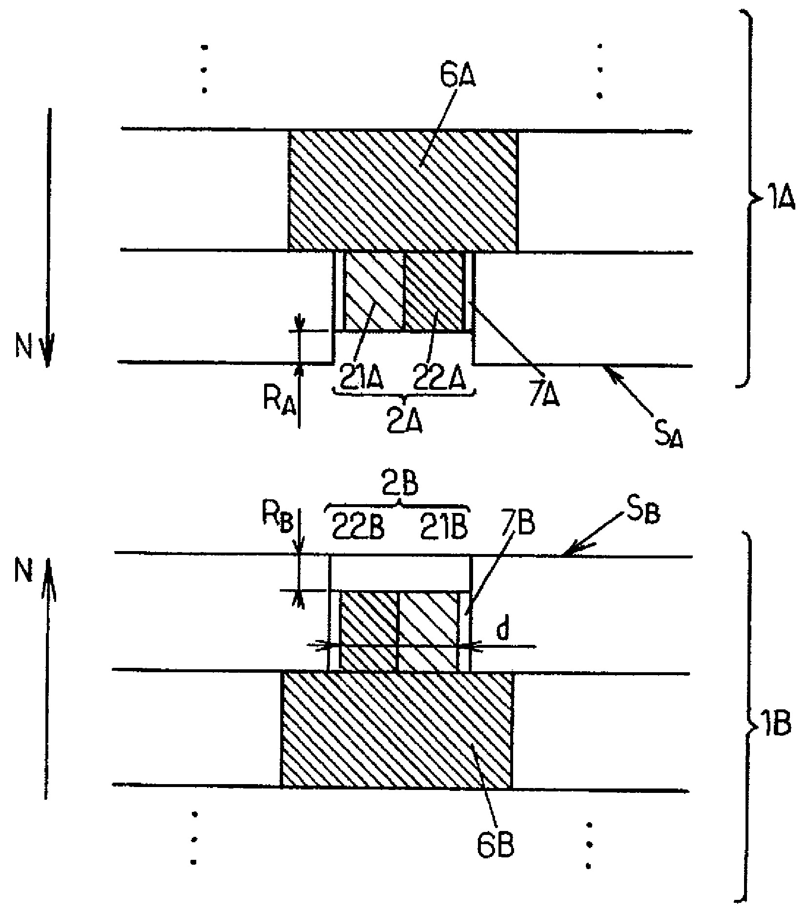
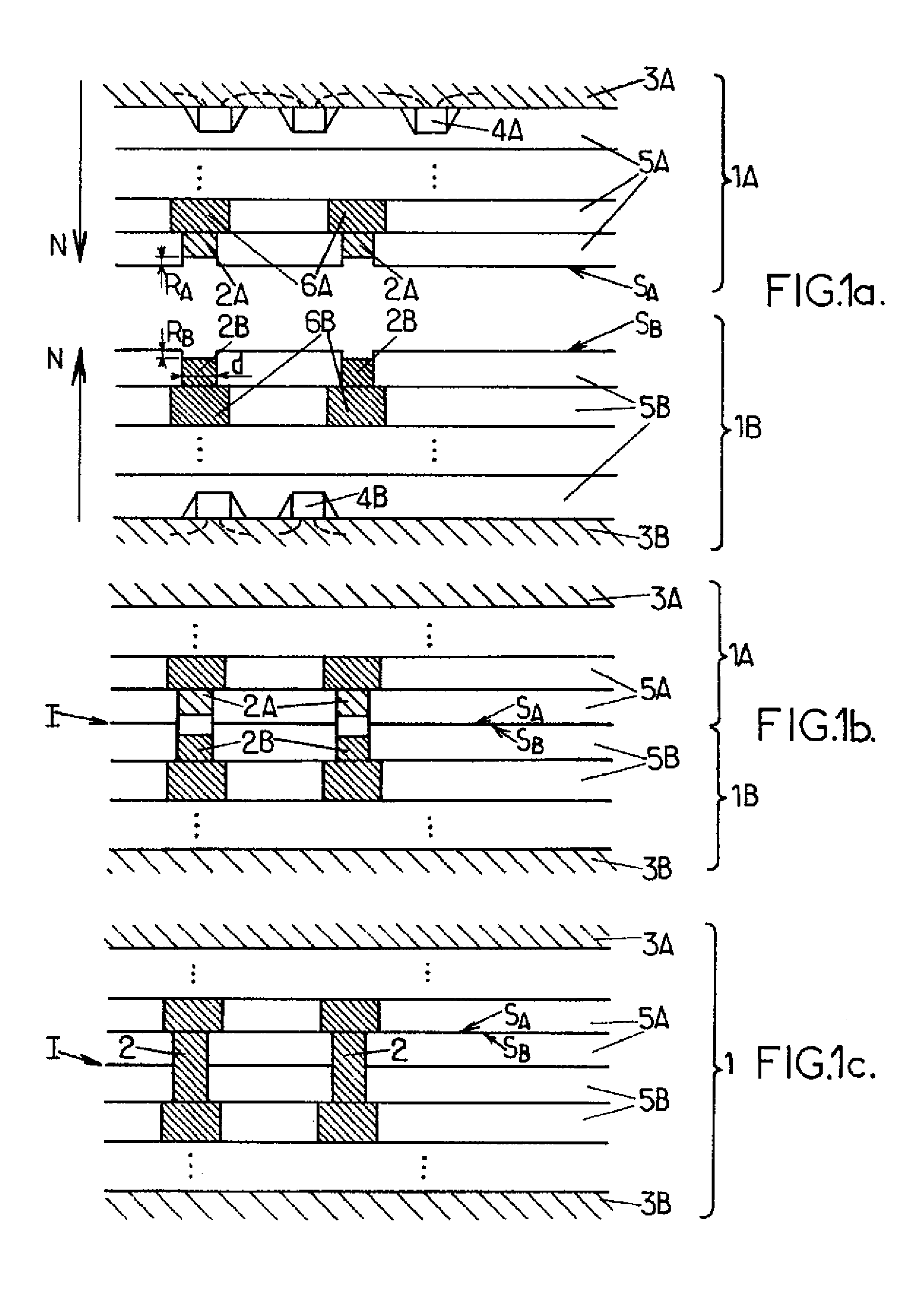
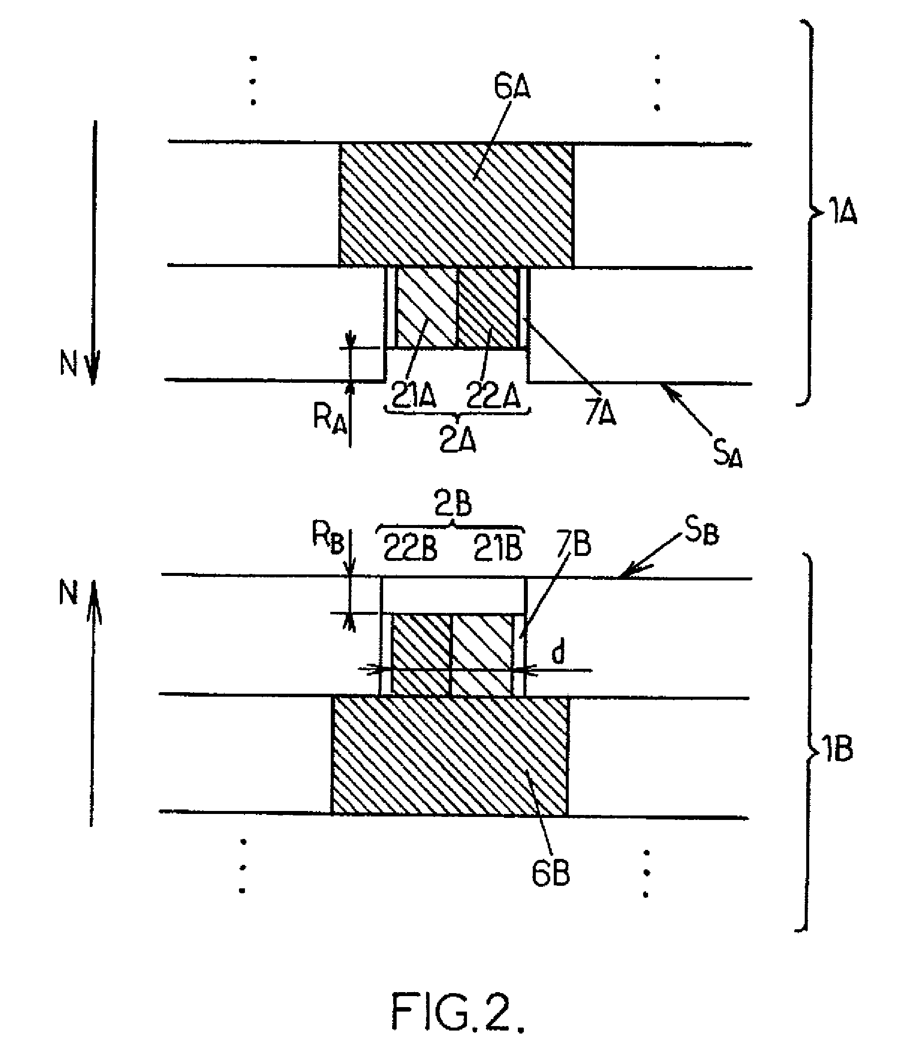
[0055]When the connection portions 2A, 2B have recesses RA, RB, the second heating may be adapted to cause at least one of the materials in the portions 2A, 2B of a same pair to diffuse across the re...


PUM

PropertyMeasurementUnit
bonding temperatureaaaaaaaaaa
temperatureaaaaaaaaaa

Abstract

A process for assembling two parts of an integrated electronic circuit has two successive steps. During a first step, the two circuit parts are made into a single unit by molecular bonding, realized on respective application surfaces of the two parts. During a second step, electrical connections are formed from connection portions already present in the application surfaces of the two circuit parts. The connections formed extend across the bonding interface, and are compatible with a high reliability and a high level of integration of the circuit.

Description

TECHNICAL FIELD[0001]This disclosure generally relates to a process for assembling two parts of an integrated electronic circuit. More particularly but not exclusively, this disclosure concerns such a process wherein an electrical connection is realized between two parts of the circuit, essentially at the circuit integration level. This disclosure also concerns a circuit of the type obtained by such a process, as well as a circuit part adapted to be assembled according to this process.BACKGROUND INFORMATION[0002]In response to the demand for increasingly complex integrated electronic circuits, System in Package circuits or SiPs have been created. Such circuits combine several circuit parts which are realized on their respective substrates and which are assembled into the same package. Each circuit part can have a different function within the complete circuit, such as an outside connection function, a random access memory function, a multimedia communication function, a digital or a...

Claims


Application Information

Patent Timeline
Patent Type & Authority Applications(United States)
IPC IPC(8): H01R9/00H05K7/00
CPCH01L25/0657Y10T29/49149H01L2225/06513H01L2225/06541H01L2924/0002H01L25/50H01L24/92H01L2224/80986H01L2224/80896H01L2224/80895H01L2224/05571H01L24/80H01L2224/9202H01L2924/01037H01L2924/01079H01L2924/00012H01L2224/05552H01L2224/80035H01L2224/80907H01L2224/80935
Inventor CORONEL, PHILIPPECOUDRAIN, PERCEVALMAZOYER, PASCALE
Owner STMICROELECTRONICS (CROLLES 2) SAS
Why Eureka
Try Eureka