Semiconductor device and a method of manufacturing the same
a manufacturing technology and integrated circuit technology, applied in semiconductor devices, semiconductor/solid-state device details, electrical devices, etc., can solve the problems of difficult to completely fill the filler in the via hole, and the anti-reflective film cannot be formed uniformly over the interlayer insulating film, so as to simplify the formation step of dual damascene. , the effect of high yield
- Summary
- Abstract
- Description
- Claims
- Application Information
AI Technical Summary
Benefits of technology
Problems solved by technology
Method used
Image
Examples
embodiment 1
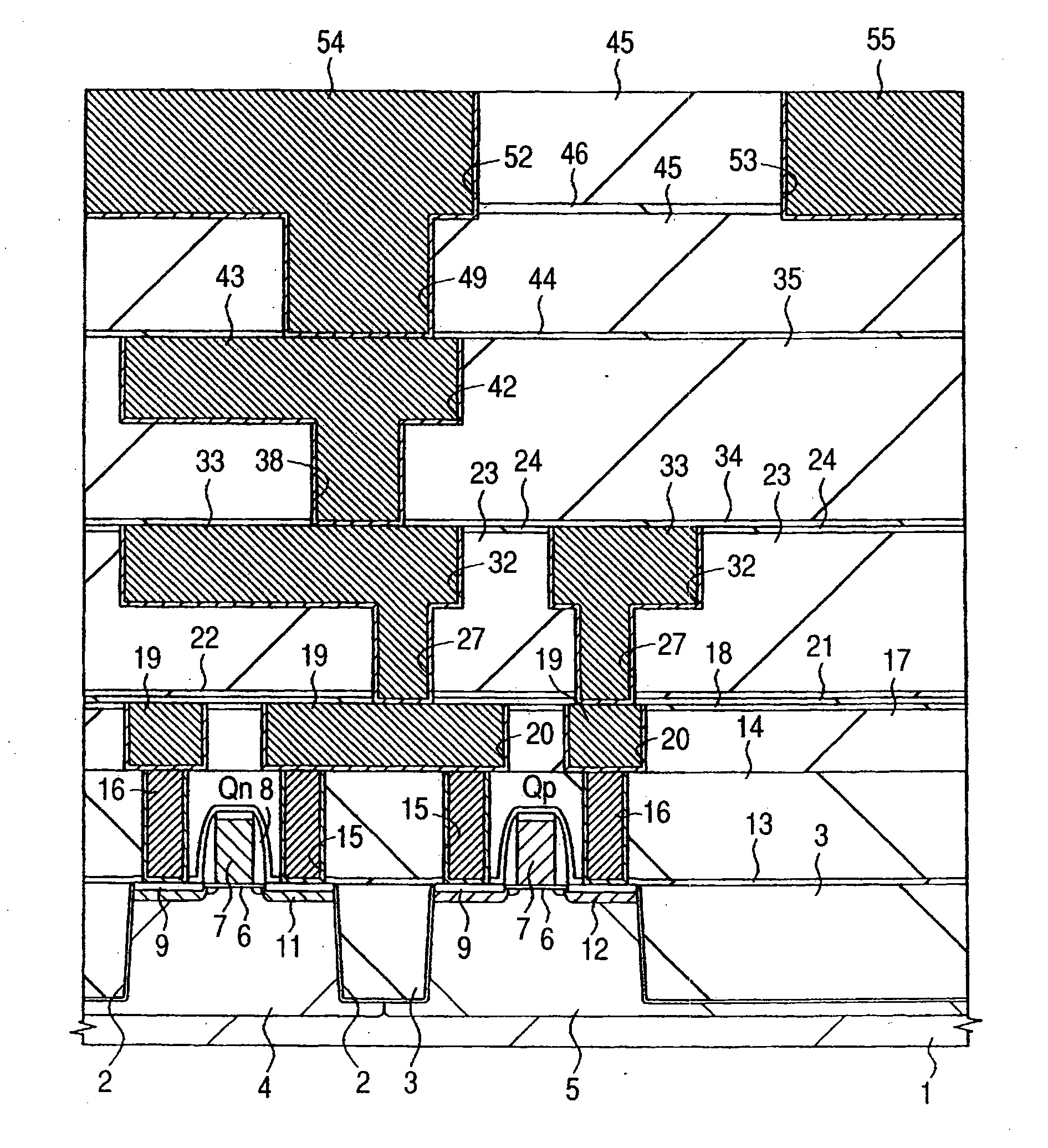
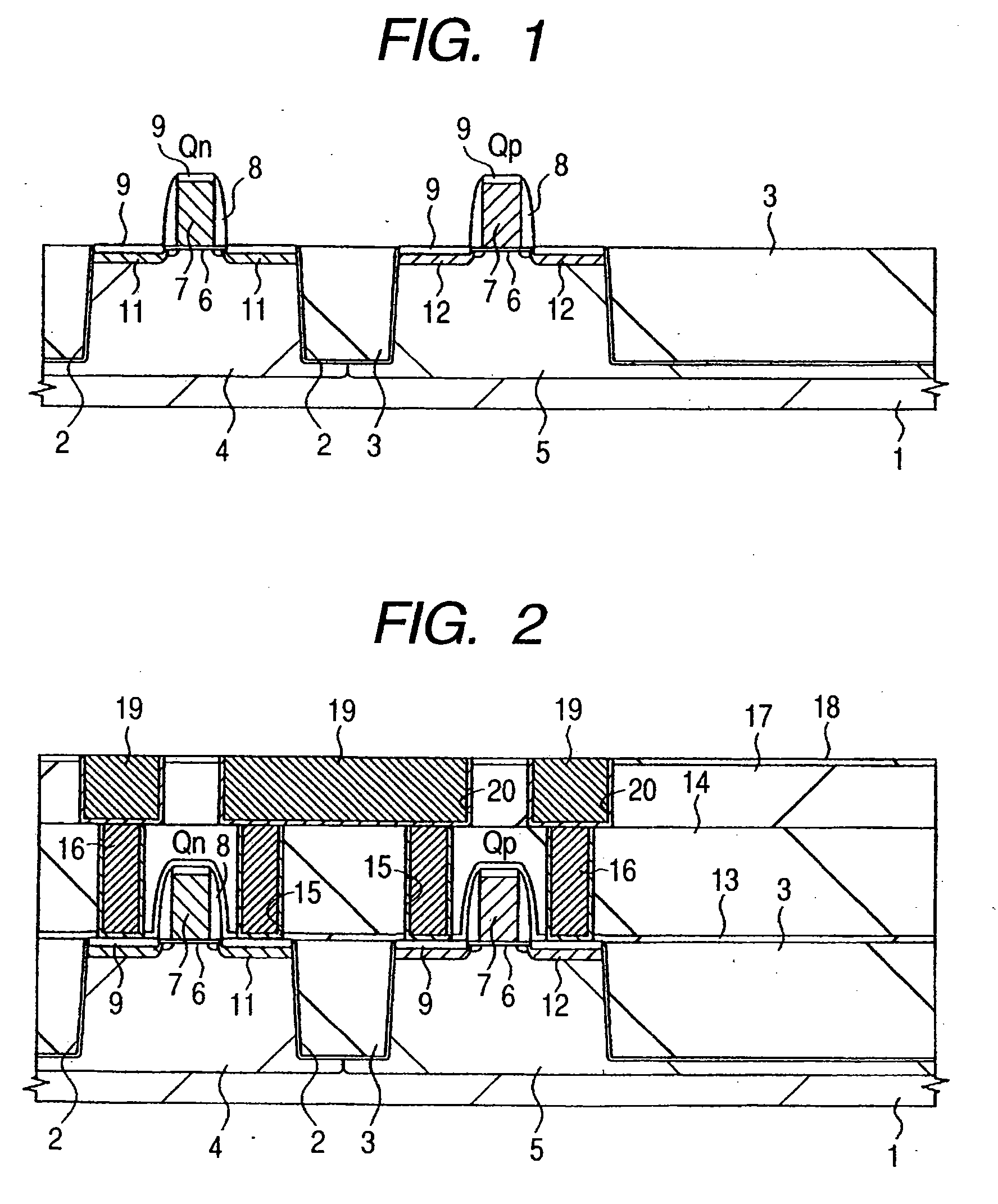
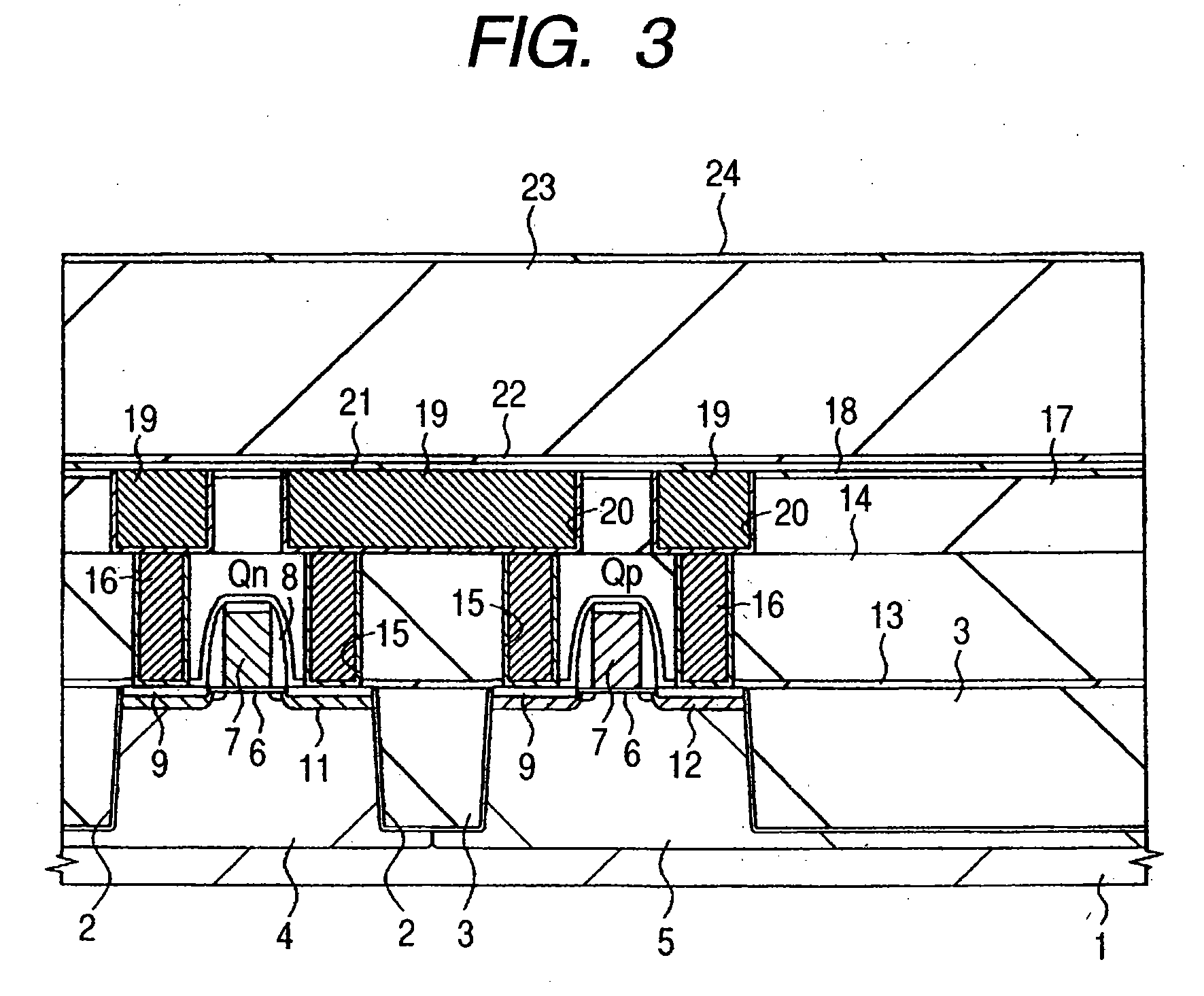
[0054]A semiconductor integrated circuit device having, for example, a four-layer Cu interconnect and fuse will be described in this Embodiment. A manufacturing method of it will next be described in the order of steps referring to FIGS. 1 to 26.
[0055]As illustrated in FIG. 1, an n channel MISFET (Qn) and a p channel MISFET (Qp) are formed as semiconductor elements over the main surface of a semiconductor substrate (which will hereinafter be called “substrate” simply), for example, made of single crystal silicon. In this drawing, indicated at numerals 2, 4 and 5 are element isolation trench, p well and n well, respectively.
[0056]The element isolation trench 2 is formed by filling an insulating film, for example, a silicon oxide film 3 in a trench formed by etching the substrate 1. The p well 4 and n well 5 are formed by ion-implanting p type impurity (boron) and n type impurity (phosphorus) into the substrate 1 and heat treating the substrate 1 to diffuse these impurities into the s...
embodiment 2
[0101]In Embodiment 1, an interconnect trench was formed after formation of a via hole in an interlayer insulating film. In this Embodiment, on the other hand, a via hole is formed after formation of an interconnect trench in an interlayer insulating film.
[0102]As illustrated in FIG. 27, a barrier insulating film 44 and an interlayer insulating film 45 are deposited over a third-level interconnect 43. A stopper film 46 is formed in the interlayer insulating film 45. An SiCN film of from about 10 nm to 100 nm thick deposited by plasma CVD is used as the stopper film 46. Steps until this step are similar to those described referring to FIGS. 1 to 15 in Embodiment 1.
[0103]As illustrated in FIG. 28, after formation of a photoresist film 51 over the interlayer insulating film 45, the interlayer insulating film 45 is dry etched with the photoresist film 51 as a mask. By stopping etching at the surface of the stopper film 46, interconnect trenches 52 and 53 are formed in the interlayer ins...
PUM
 Abstract
Description
Claims
Application Information


