
Method and apparatus for a dynamic semiconductor memory with compact sense amplifier circuit

Inactive Publication Date: 2008-09-11
BREEN KRISTOPHER CHAD +1
View PDF6 Cites 10 Cited by
  • Summary
  • Abstract
  • Description
  • Claims
  • Application Information

AI Technical Summary

Benefits of technology

[0030](c) an architecture that enables said column read / write circuits to function as intended while maintaining a high density of components within the memory device.
[0037]The memory device has higher density but lower speed than conventional dynamic memories, making it suitable for applications that require a low cost memory but have flexible speed requirements. Such applications include, but are not limited to, file memory for tertiary storage in a computer system, portable solid-state disk, and low-latency standalone network devices.

Problems solved by technology

It offers good read and write performance, but consumes a fairly substantial amount of power compared with other memories.
Non-volatile memories, in general, have reasonably high density, and often have similar read performance to DRAM; however, most presently available rewritable non-volatile memories have poor write performance.
Furthermore, they are only capable of a limited number of rewrites, which prevents them from competing with DRAM as an inexpensive, well-performing memory for computing systems.
When a cell was selected and a signal was transferred to the “read” bitline, the sense transistor would drive a near zero current to an output pin to indicate a logic “high” or a 400-μA current to indicate a logic “low.” Today, single-ended sensing is used very little, since it does not allow sufficient performance for most modern memories.
This sharing of a single sense amplifier between a group of bitlines significantly reduces the sense amplifier area in a DRAM, which in turn reduces the area of the DRAM chip as a whole.

Method used


Image

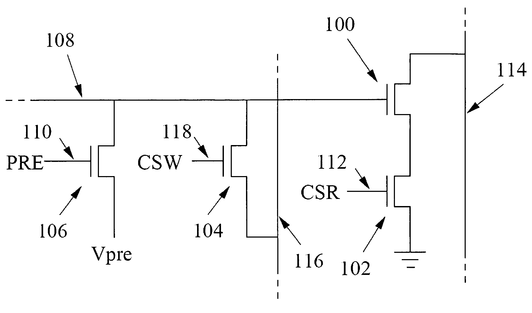
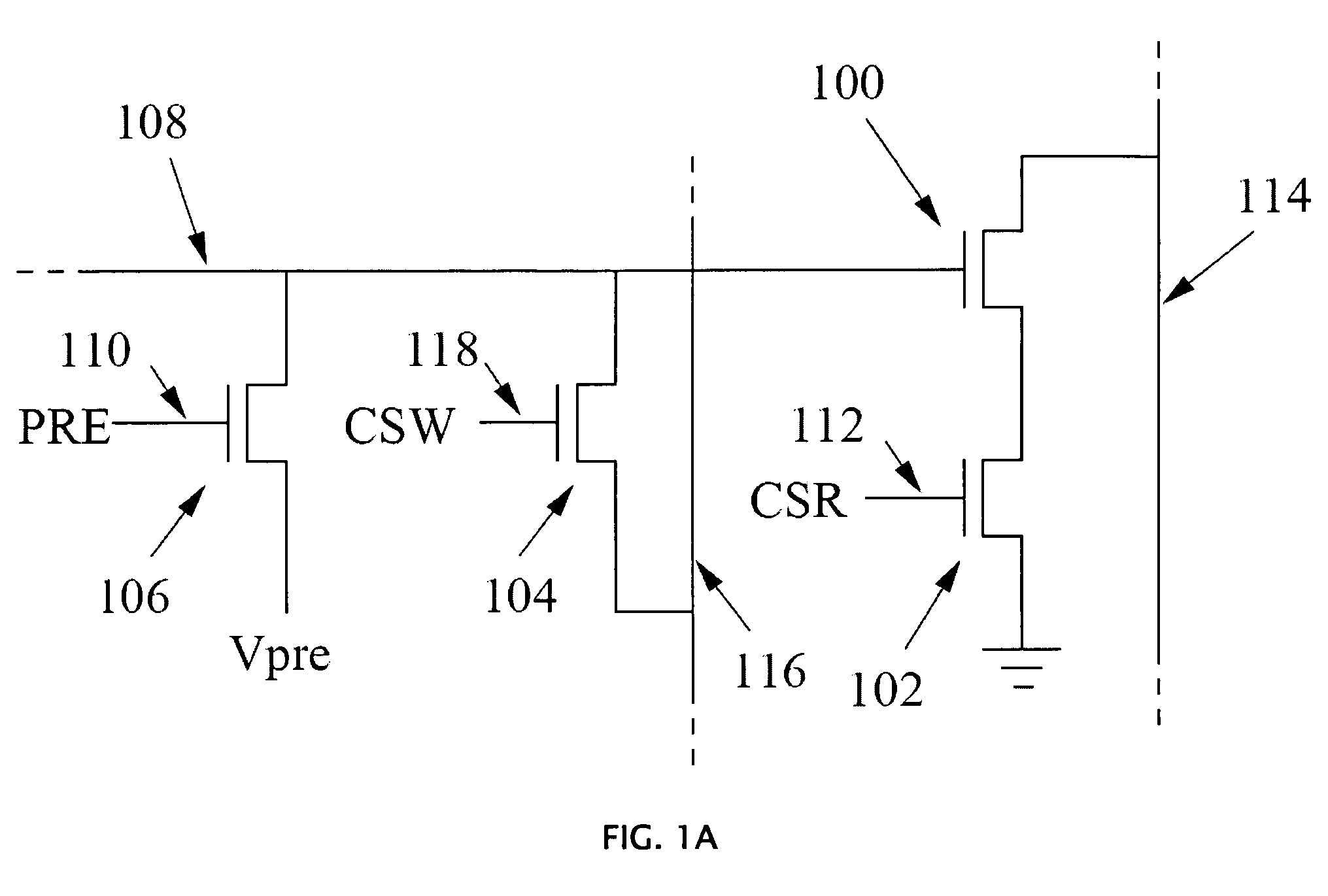
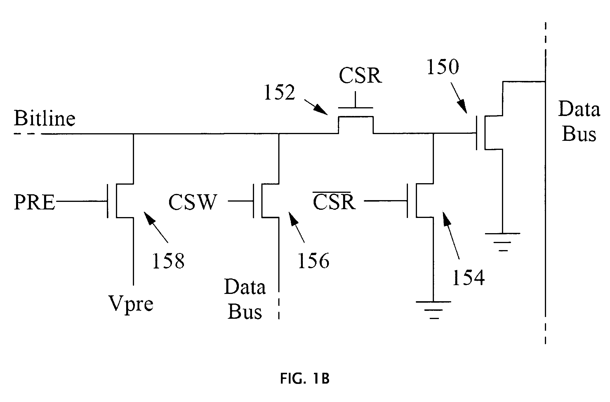
  • Method and apparatus for a dynamic semiconductor memory with compact sense amplifier circuit
  • Method and apparatus for a dynamic semiconductor memory with compact sense amplifier circuit
  • Method and apparatus for a dynamic semiconductor memory with compact sense amplifier circuit

Examples


Embodiment Construction

[0056]The present invention is a dynamic memory device that comprises a new architecture, circuitry, and method for data storage and retrieval. The device provides a higher-density memory compared with conventional DRAM. It is enabled by the use of very small, simple sense amplifiers, as well as an open bitline array organization. A number of novel techniques are presented for coping with reduced-complexity sense amplifiers, as well as for improving the economics of the memory. Such techniques include reducing bitline length, adding separate read and write select lines, using a two-pass write operation to reduce coupling noise, allowing for serial I / O, and employing a unique reference scheme.

General Operation

[0057]Within the memory array are typical dynamic storage cells that operate identically to the cells in DRAM. When a sub-row of data, which constitutes a single block unit of sequential data, is to be read from a sub-array, the sub-wordline corresponding to that sub-row is acti...


PUM


Abstract

A high-density dynamic memory device with compact sense amplifier circuit is described. The memory device achieves high density through the use of a compact sense amplifier circuit that employs a single transistor to sense stored dynamic data. Functionality of the device is enabled by an architecture and method of operation that support a compact sense amplifier circuit. Enabling techniques include sequential sensing of memory columns, a two-pass write operation, a two-step refresh operation, a reference scheme that uses reference data stored in regular memory cells, and the application of digital signal processing to determine sensed data and cancel crosstalk noise.

Description

U.S. PATENTS CITED[0001]Robert H. Dennard, Field-Effect Transistor Memory, 1968, U.S. Pat. No. 3,387,286.[0002]Robert F. Harland, MOS One Transistor Cell RAM Having Divided and Balanced Bit Lines, Coupled by Regenerative Flip-Flop Sense Amplifiers, and Balanced Access Circuitry, 1977, U.S. Pat. No. 4,045,783.[0003]Toshiaki Kirihata et al., Destructive Read Architecture for Dynamic Random Access Memories, 2004, U.S. Pat. No. 6,829,682.FIELD OF THE INVENTION[0004]This invention relates to integrated memory circuits and more particularly to high-density dynamic memory with compact sense amplifier circuitry.BACKGROUND OF THE INVENTION[0005]Semiconductor memories can be generally divided into two broad categories based on their volatility, or ability to retain data in the absence of supplied power. Volatile memory can be sub-classified based on the method of data retention used, dynamic or static. Dynamic volatile memory, known as Dynamic Random Access Memory (DRAM), requires periodic re...

Claims


Application Information

Patent Timeline
IPC IPC(8): G11C7/06
CPCG11C11/4094G11C11/4091
Inventor BREEN, KRISTOPHER CHADELLIOTT, DUNCAN GEORGE
Owner BREEN KRISTOPHER CHAD
Learn More