Semiconductor device, semiconductor display device, and manufacturing method of semiconductor device

Inactive Publication Date: 2008-09-18
SEMICON ENERGY LAB CO LTD
View PDF31 Cites 25 Cited by
  • Summary
  • Abstract
  • Description
  • Claims
  • Application Information

AI Technical Summary

Benefits of technology

[0030]According to the present invention, by employing crystal faces and/or crystal axes with which mobility of carriers flowing through channels of MISFETs becomes high, carrier effective mass can be the smallest; accordingly, carrier effective mobility can be the highest. Therefore, high speed operation of a semiconductor device can be achieved. Further, low voltage driving of the semiconductor device becomes possible, and low power consumption can be achieved.
[0031]By making the n-channel MISFET and the p-channel MISFET have at least different crystal faces or crystal axes, a s

Problems solved by technology

However, it is said that improvement in performance of semiconductor integrated circuits by miniaturization has a limit.
Therefore, there is also a limit from an economic perspective.
In addition, a light-transmitting property is low due to

Method used


Image

  • Semiconductor device, semiconductor display device, and manufacturing method of semiconductor device
  • Semiconductor device, semiconductor display device, and manufacturing method of semiconductor device
  • Semiconductor device, semiconductor display device, and manufacturing method of semiconductor device

Examples


embodiment mode 1

[0068]Embodiment Mode 1 will describe a mode of transferring semiconductor layers which form an n-channel MISFET and a p-channel MISFET from single-crystalline semiconductor substrates having different crystal faces (hereinafter also referred to as bond wafers) to the same surface of a substrate having an insulating surface (hereinafter also referred to as a base substrate). A mode where crystal faces with which mobility of carriers moving in channel length directions is increased are employed for an n-channel MISFET and a p-channel MISFET, that is, a mode where a semiconductor layer whose crystal face is {100} is employed for the n-channel MISFET and a semiconductor layer whose crystal face is {110} is employed for the p-channel MISFET will be described below.

[0069]In order to obtain a single-crystalline semiconductor layer for forming a channel formation region, a source region, and a drain region in the n-channel MISFET, a bond wafer whose crystal face is {100} is used. In order ...

embodiment mode 2

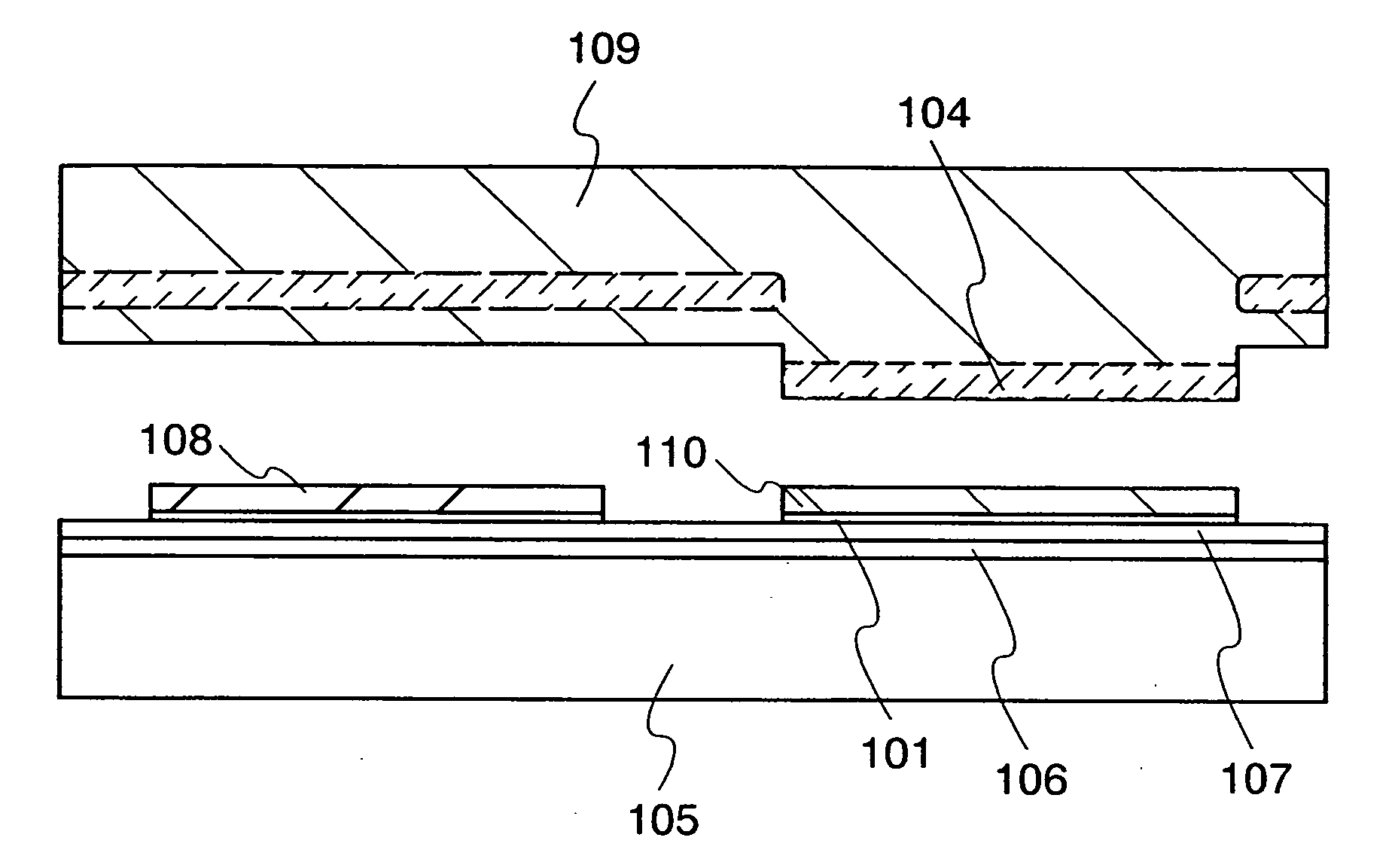
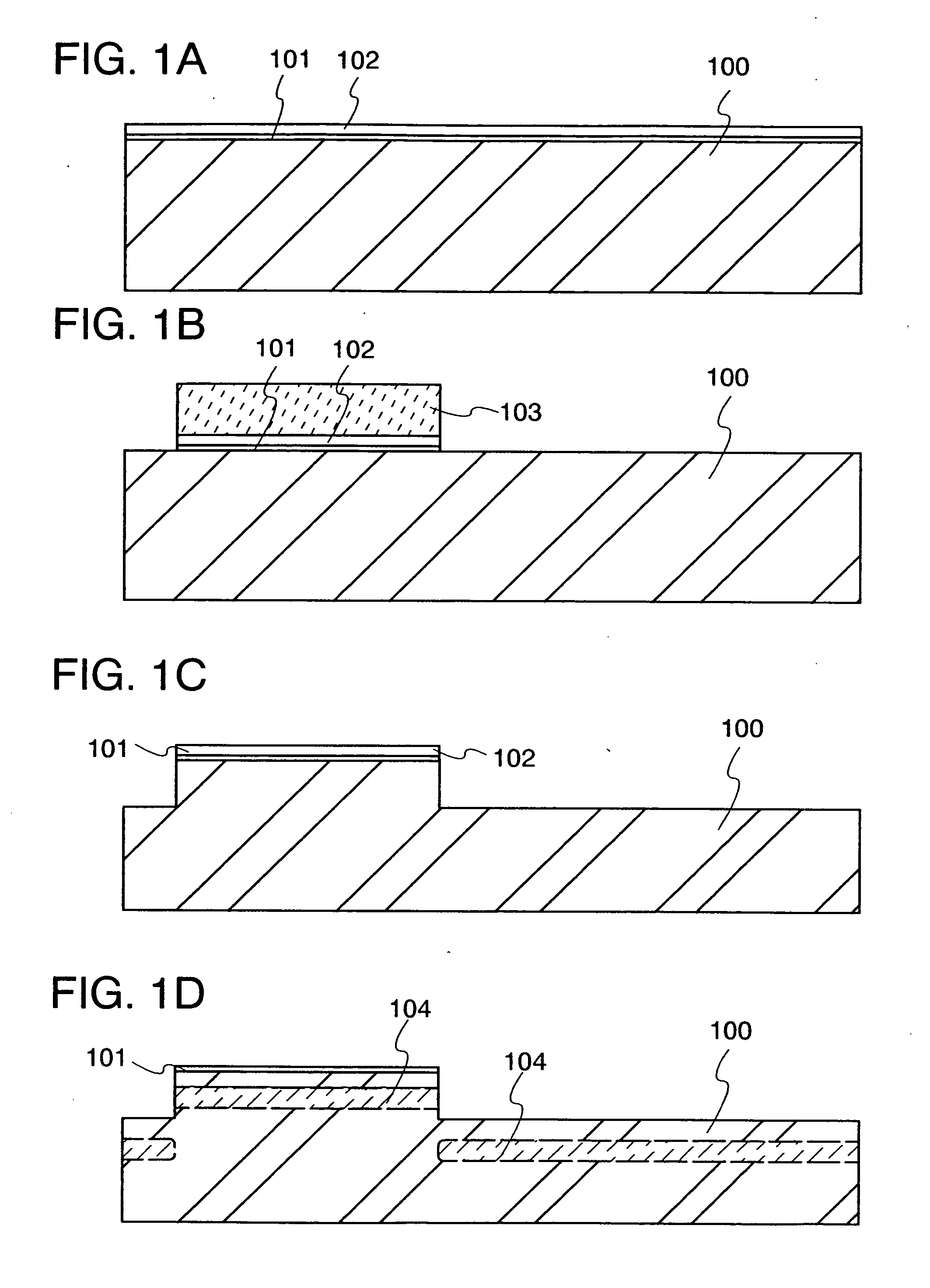
[0084]Embodiment Mode 2 describes a manufacturing process of a bond wafer different from the process shown in FIGS. 1A to 1D, with reference to FIGS. 4A and 4B. In FIG. 4A, a silicon oxide film 101 and a silicon nitride film 102 are formed over a surface of a first bond wafer 100. Then, ions of hydrogen, a rare gas, or both of hydrogen and a rare gas are added, so that a fragile layer 104 is formed in the first bond wafer 100. Next, formation of a groove is conducted as shown in FIG. 4B. In the formation of the groove, the groove is processed to be deeper than the fragile layer 104, so that the fragile layer 104 can remain only in a region of a single-crystalline semiconductor layer which should be transferred. With this structure, transfer can be easily performed.

embodiment mode 3

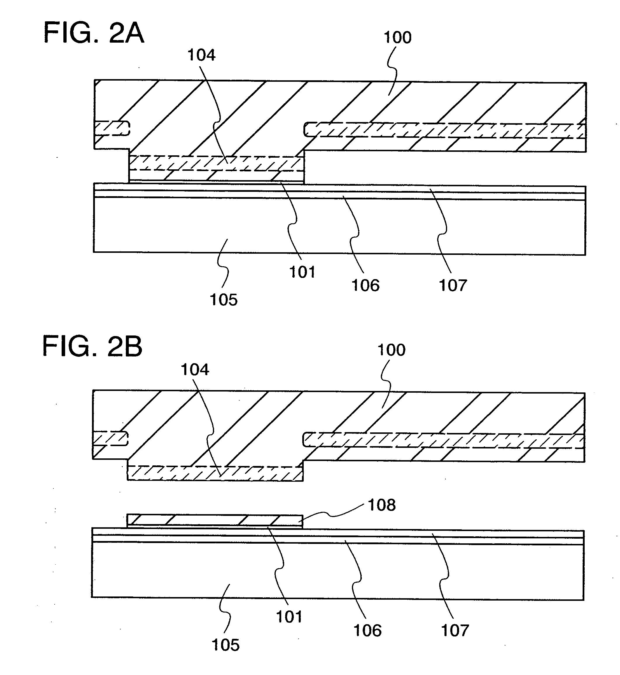
[0085]Embodiment Mode 3 will describe a manufacturing method of a semiconductor element substrate, in which SOI layers for forming an n-channel MISFET and a p-channel MISFET are transferred from respective bond wafers whose crystal faces are different to the same surface of a base substrate that is a light-transmitting insulating substrate different from the bond wafers. In this embodiment mode, a bond wafer whose crystal face is {100} is used for an n-channel MISFET, and a channel formation region, a source region, and a drain region are formed. Further, a bond wafer whose crystal face is {110} is used for a p-channel MISFET, and a channel formation region, a source region, and a drain region are formed. In this embodiment mode, description is made in the order in which the SOI layer of the n-channel MISFET is transferred to the light-transmitting insulating substrate and then the SOI layer of the p-channel MISFET is transferred to the insulating substrate; however, either of the S...


PUM


Abstract

To achieve high performance of a semiconductor integrated circuit depending on not only a microfabrication technique but also another way. In addition, to achieve low power consumption of a semiconductor integrated circuit. A semiconductor device is provided in which crystal faces and/or crystal axes of single-crystalline semiconductor layers of a first conductive MISFET and a second conductive MISFET are different. The crystal faces and/or crystal axes are arranged so that mobility of carriers flowing in channel length directions in the respective MISFETs is increased. Such a structure can increase mobility of carriers flowing through channels of the MISFETs and high speed operation of a semiconductor integrated circuit can be achieved. Further, low voltage driving becomes possible, and low power consumption can be realized.

Description

BACKGROUND OF THE INVENTION[0001]1. Field of the Invention[0002]The present invention relates to a semiconductor device having a so-called SOI (silicon on insulator) structure in which a semiconductor layer is provided on an insulating surface. Further, the present invention relates to a semiconductor display device having an SOI structure on an insulating substrate having a light-transmitting property such as a glass substrate, and a manufacturing method thereof.[0003]2. Description of the Related Art[0004]Integrated circuits using semiconductor substrates called silicon on insulator (hereinafter also referred to as “SOI”) in which a single-crystalline semiconductor layer is formed on an insulating surface instead of using silicon wafers that are manufactured by thinly slicing an ingot of single-crystalline semiconductor are developed. The integrated circuits using the SOI substrates draw attention as semiconductor integrated circuits whose performance is improved by reduction of p...

Claims


Application Information

Patent Timeline
IPC IPC(8): H01L21/30H01L29/04
CPCH01L21/2007H01L21/76254H01L29/785H01L29/045H01L27/1203H01L21/20
Inventor YAMAZAKI, SHUNPEIMIYAIRI, HIDEKAZU
Owner SEMICON ENERGY LAB CO LTD
Why Eureka
Try Eureka