Method to form a pattern of functional material on a substrate by treating a surface of a stamp
a functional material and stamping technology, applied in the field of photolithography, can solve the problems of incompatible with reel-to-reel processes, complex multi-step processes, and inability to print plastic electronics,
- Summary
- Abstract
- Description
- Claims
- Application Information
AI Technical Summary
Benefits of technology
Problems solved by technology
Method used
Image
Examples
example 1
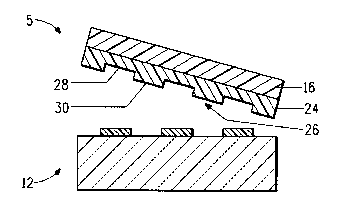
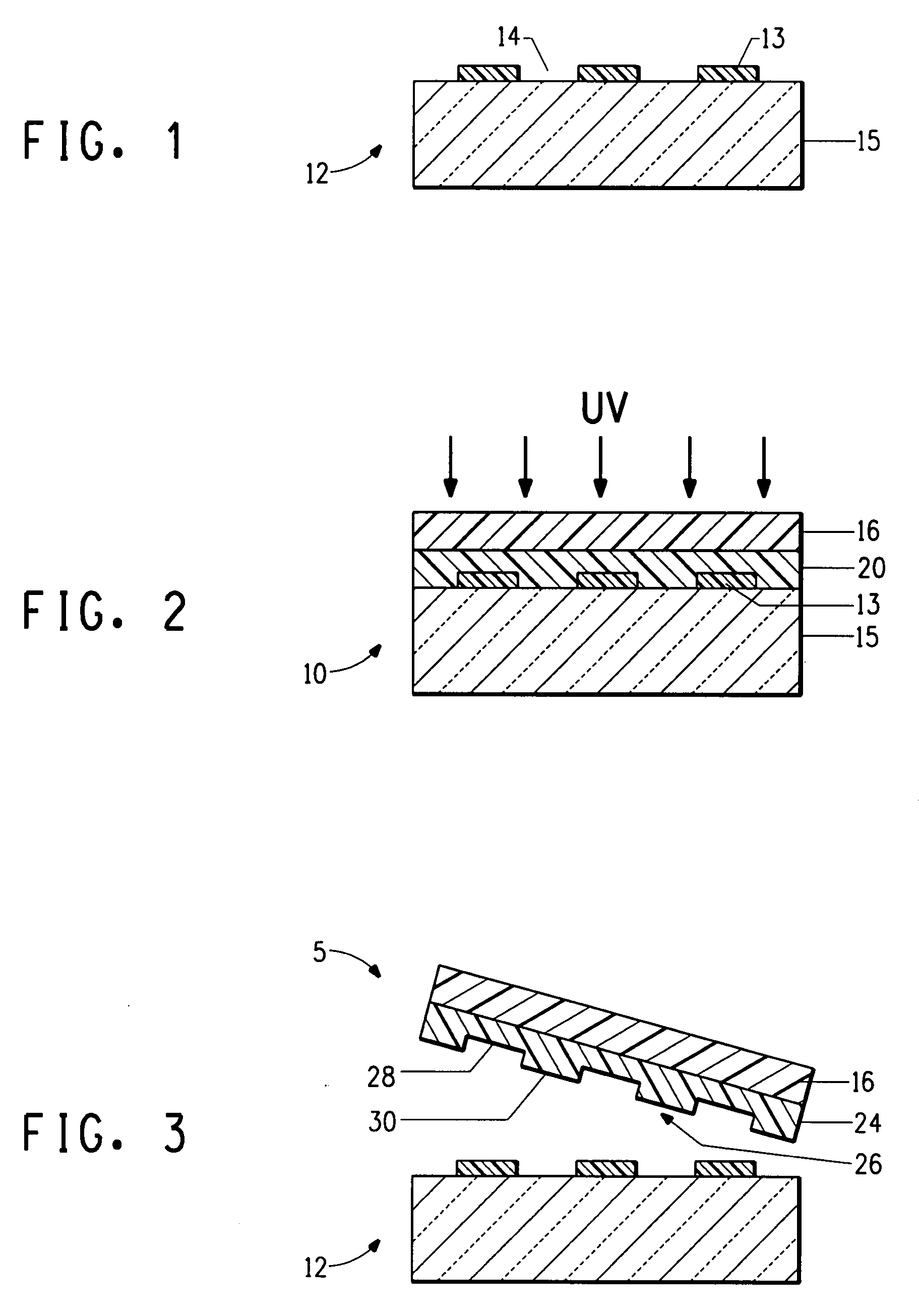
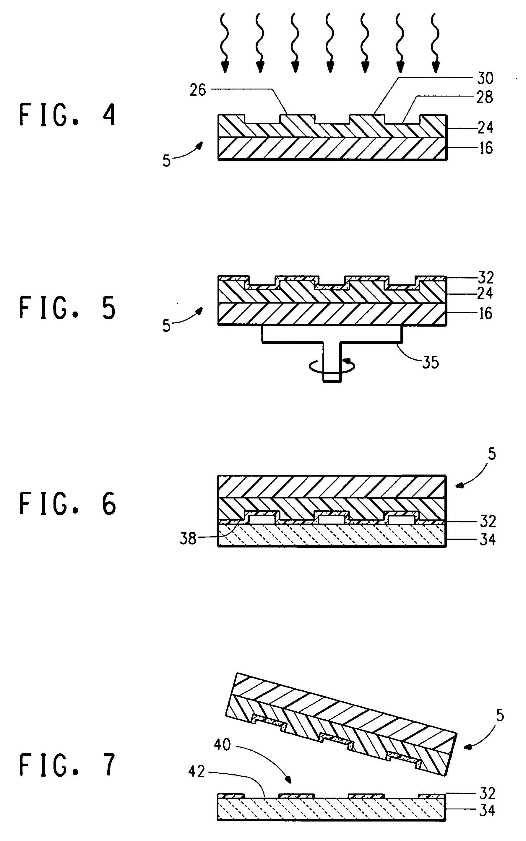
[0072]The following example demonstrates the printing of a high resolution, high conductivity silver pattern onto a flexible substrate using an elastomeric polyfluoropolyether (PFPE) stamp having a relief structure that was plasma treated to enhance its surface wetting capability.
Master Preparation:
[0073]A 0.6 micrometer thick layer of a negative photoresist, SU-8 type 2 (from MicroChem, Newton, Mass.) was coated onto a silicon wafer at 3000 rpm for 60 sec. The wafer with the coated photoresist film was heated 65° C. for 1 minute and then baked at 95° C. for 1 minute to fully dry the film. The baked film was then exposed for 5 sec in I-liner (OAI Mask Aligner, Model 200) at 365 nm through a mask having a pattern of lines and spaces and rectangles with dimensions varying from 5 to 250 micron, and post-baked at 65° C. for 1 min. After a final bake at 95° C. for 1 minute the non-exposed photoresist was developed in SU-8 developer for 1 minute. The developed film was dried with nitrogen...
example 2
[0089]Example 1 was repeated except that the flexible substrate was not coated with the adhesive, i.e., the flexible substrate did not include the adhesive layer.
[0090]The silver functional material on the elastomeric stamp was printed by contact transfer of the uppermost surface of the raised portions of the relief onto the Melinex® 561 polyester film without latex adhesive layer. The silver material was spin coated onto the relief surface of the stamp, but not completely dried (some solvent remained in the silver composition) before the stamp was contacted to the substrate. The silver pattern was transferred by placing the relief surface of the stamp coated with the silver film onto the flexible substrate which was placed on a hot plate at 65° C., and applying gentle pressure to the support side of the stamp. The stamp was separated from the substrate to form a partial pattern of the silver film on the substrate.
[0091]Although the silver pattern did not transfer completely onto th...
PUM
| Property | Measurement | Unit |
|---|---|---|
| thickness | aaaaa | aaaaa |
| temperature | aaaaa | aaaaa |
| height | aaaaa | aaaaa |
Abstract
Description
Claims
Application Information


