Oxidized Barrier Layer

a barrier layer and oxidized technology, applied in the direction of vacuum evaporation coating, semiconductor/solid-state device details, coatings, etc., can solve the problems of increasing the conductivity of the integrated circuit, the fabrication and reliable operation of the integrated circuit requires a more complex structure, and the reliability problem is increased

Inactive Publication Date: 2008-10-02
APPLIED MATERIALS INC
View PDF7 Cites 43 Cited by
  • Summary
  • Abstract
  • Description
  • Claims
  • Application Information

AI Technical Summary

Problems solved by technology

However, a more complex structure is required for the fabrication and reliable operation of a integrated circuit incorporating copper metallization.
A barrier is required between the copper to be filled into the via and the dielectric material to prevent the migration of copper into the dielectric, which would increase its conductivity and create a reliability problem.
However, the challenges continue to mount as the via widths decrease and the aspect ratio of the vias increase.
These problems arise in part by the requirement that the barrier layers be relatively thin, for example, a few nanometers as the via widths decrease to well below 40 nm.
However, a sputtered tantalum ruthenium barrier presents problems of its own.

Method used


Image

  • Oxidized Barrier Layer
  • Oxidized Barrier Layer
  • Oxidized Barrier Layer

Examples


Embodiment Construction

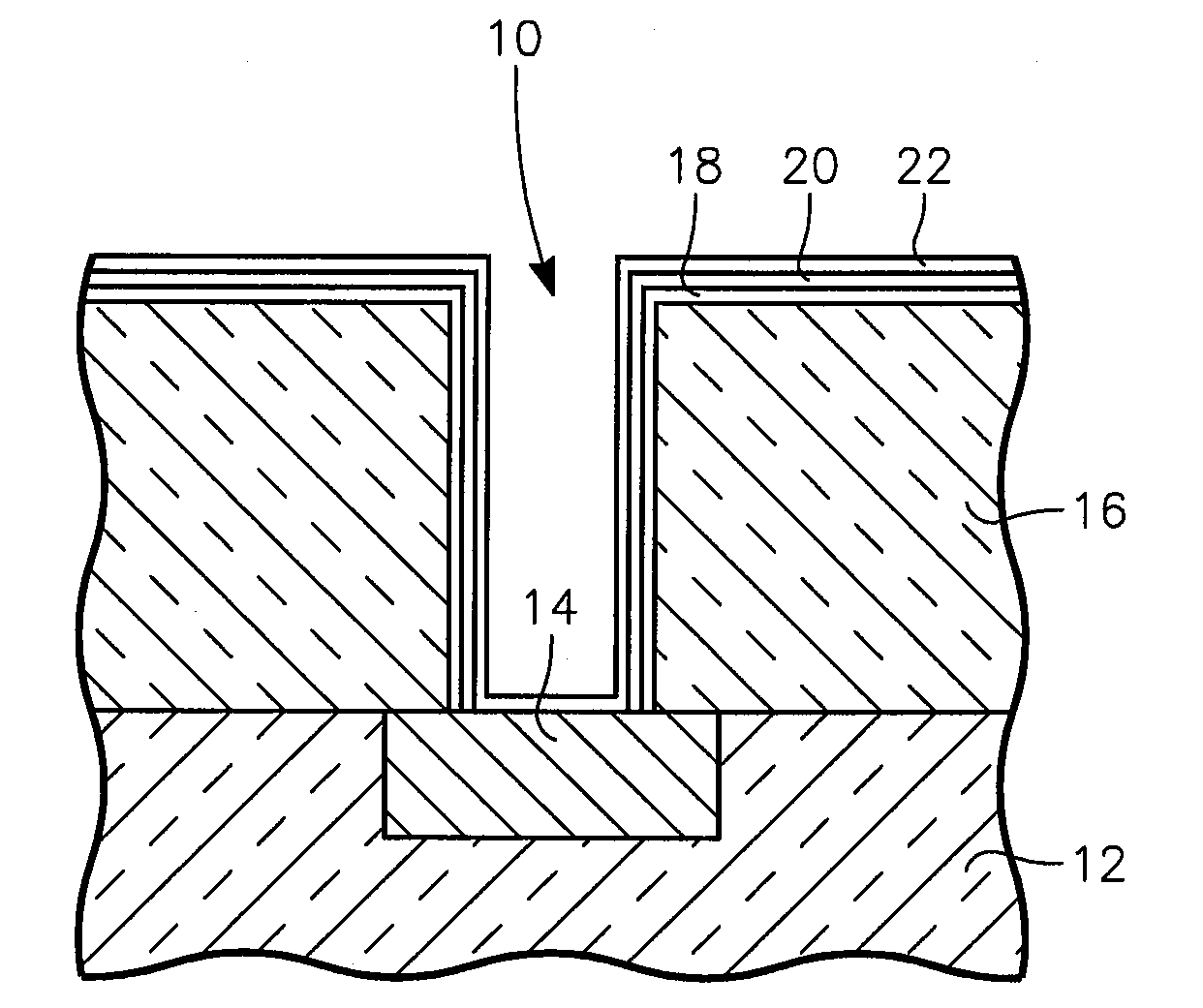
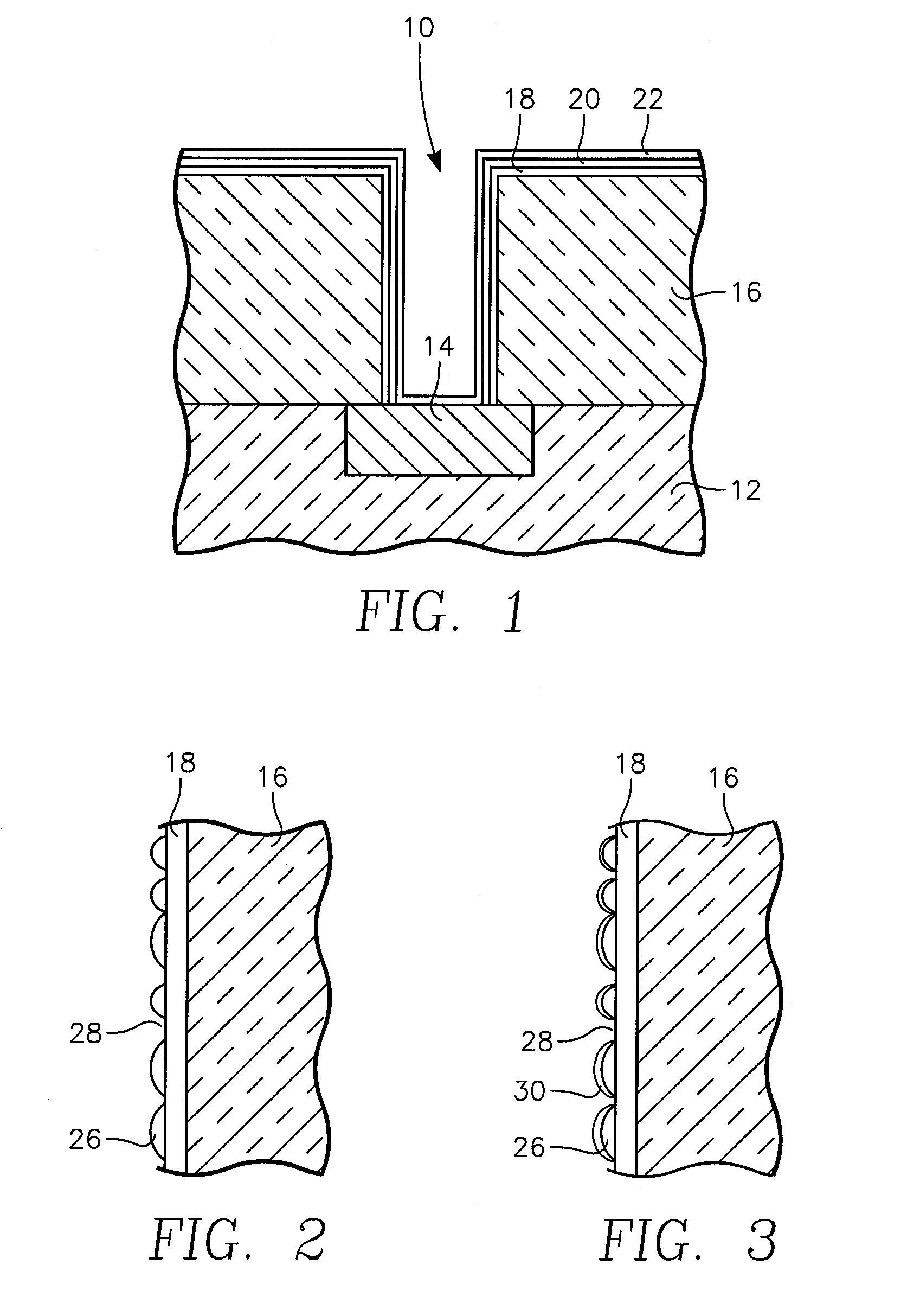
[0027]We have observed that thin layers of ruthenium tantalum tend to deposit on the sidewalls of the vias to have a roughened surface. Pure tantalum seems to sputter deposit with a smoother surface than ruthenium tantalum. In the extreme, as illustrated in the cross-sectional view of FIG. 2, ruthenium tantalum deposits on the ruthenium tantalum nitride layer 18 as isolated RuTa islands 26 with gaps 28 between them. When copper is then sputter deposited, although some of it lands on the ruthenium tantalum nitride layer 18, it does not well adhere to the nitride material but instead forms a poor, possibly discontinuous copper seed layer 30 is formed, as illustrated in FIG. 3, with some of the gaps 28 remaining to expose the underlying ruthenium tantalum nitride layer 18. As a result, when copper is electroplated to fill the remainder of the via hole 10, the gaps in the copper seed layer 30 may interrupt the electroplating current and the exposed ruthenium tantalum nitride does not we...


PUM

PropertyMeasurementUnit
thicknessaaaaaaaaaa
pressureaaaaaaaaaa
dielectricaaaaaaaaaa

Abstract

A method and resultant produce of forming barrier layer based on ruthenium tantalum in a via or other vertical interconnect structure through a dielectric layer in a multi-level metallization. The RuTa layer in a RuTa / RuTaN bilayer, which may form discontinuous islands, is actively oxidized, preferably in an oxygen plasma, to thereby bridge the gaps between the islands. Alternatively, ruthenium tantalum oxide is reactive sputtered onto the RuTaN or directly onto the underlying dielectric by plasma sputtering a RuTa target in the presence of oxygen.

Description

FIELD OF THE INVENTION[0001]The invention relates generally to sputter deposition in the formation of integrated circuits. In particular, the invention relates to sputter deposition of barrier layers in inter-level interconnects.BACKGROUND ART[0002]Advanced integrated circuits include multiple levels of wiring separated by inter-level dielectric layers. Vias are etched in the dielectric layers and are filled with a metallization to vertically connect the different levels of horizontal interconnections. Currently copper is the preferred metallization metal and is often used in dual-damascene interconnect structure in which the dielectric layer is etched in a two-step process to have narrow vertically extending vias etched in the lower part of the dielectric layer and wider horizontally extending trenches etched in the upper part of the dielectric layer typically interconnecting different ones of the vias. Copper is then filled into both the vias and trenches by electrochemical platin...

Claims


Application Information

Patent Timeline
Patent Type & Authority Applications(United States)
IPC IPC(8): C23C14/34
CPCC23C14/046C23C14/0036C23C14/0641C23C14/083H01L21/2855H01L21/76844H01L21/76846H01L21/76856H01L21/76868H01L23/53238H01L2924/0002
Inventor TANG, XIANMINCHUNG, HUAWANG, RONGJUNGOPALRAJA, PRABURAMYU, JICK M.WANG, JENN YUE
Owner APPLIED MATERIALS INC
Why Eureka
Try Eureka