Method for manufacturing semiconductor device, semiconductor device, semiconductor circuit, electro-optical device, and electronic apparatus

a manufacturing method and semiconductor technology, applied in semiconductor devices, solid-state devices, thermoelectric devices, etc., can solve the problems of deterioration of tft characteristics in the atmosphere, gate insulation layer becomes difficult to dissolve in solvent, gate insulation layer cannot be formed, etc., to achieve high performance, semiconductor circuits high performance, and superior semiconductor characteristics

Active Publication Date: 2008-10-02
E INK CORPORATION
View PDF10 Cites 22 Cited by
  • Summary
  • Abstract
  • Description
  • Claims
  • Application Information

AI Technical Summary

Benefits of technology

[0015]An advantage of the invention is to provide a semiconductor device superior in semiconductor characteristics without causing dielectric breakdown, a method for securely manufacturing the semiconductor device, a high performance semiconductor circuit provided with the semiconductor device, a high performance electro-optical device provided with the same, and a highly reliable electronic apparatus.
[0016]The above advantage is attained by following aspects of the invention.
[0017]A method for manufacturing a semiconductor device according to a first aspect of the invention includes: forming a source electrode and a drain electrode on a substrate; forming an organic semiconductor layer including a n conjugated organic compound at least between the source electrode and the drain electrode; applying an application liquid on the organic semiconductor layer, the application liquid being made of a polymer of an alicyclic compound dissolved in a paraffin hydrocarbon solvent that is a carbocyclic compound without having aromaticity; forming a gate insulation layer including the polymer of the alicyclic compound by removing the paraffin hydrocarbon solvent from the application liquid; and forming a gate electrode on the gate insulation layer.
[0018]The gate insulation layer can thus include a nonpolar substance and a nonpolar solvent, preventing an organic semiconductor material and a gate electrode material from diffusing into the gate insulation layer. As a result, a semiconductor device not causing dielectric breakdown, but having excellent semiconductor characteristics can be easily and securely obtained.
[0019]A method for manufacturing a semiconductor device according to a second aspect of the invention includes: forming a gate electrode on a substrate; applying an application liquid on the substrate so as to cover the gate electrode, the application liquid being made of a polymer of an alicyclic compound dissolved in a paraffin hydrocarbon solvent that is a carbocyclic compound without having aromaticity; forming a gate insulation layer including the polymer of the alicyclic compound by removing the paraffin hydrocarbon solvent from the application liquid; forming an organic semiconductor layer including a π conjugated organic compound on the gate insulation layer; and forming a source electrode and a drain electrode on the organic semiconductor layer.
[0020]The gate insulation layer can thus include a nonpolar substance and a nonpolar solvent, preventing an organic semiconductor material and a gate electrode material from diffusing into the gate insulation layer. As a result, a semiconductor device not causing dielectric breakdown, but having excellent semiconductor characteristics can be easily and securely obtained.

Problems solved by technology

If polymethyl methacrylate (hereinafter, abbreviated as “PMMA”) is used as the material forming a gate insulation layer, high hygroscopicity of PMMA causes deterioration of the TFT characteristics in the atmosphere.
Further, if a polymer that has high heat resistance is used as the material forming a gate insulation layer, the gate insulation layer becomes hard to dissolve in a solvent because the polymer has rigidity.
As a result, the gate insulation layer cannot be formed.
However, the gate insulation layer made thin has a high incidence of dielectric breakdown, thereby having an issue in which devices lack reliability.

Method used


Image

  • Method for manufacturing semiconductor device, semiconductor device, semiconductor circuit, electro-optical device, and electronic apparatus
  • Method for manufacturing semiconductor device, semiconductor device, semiconductor circuit, electro-optical device, and electronic apparatus
  • Method for manufacturing semiconductor device, semiconductor device, semiconductor circuit, electro-optical device, and electronic apparatus

Examples


first embodiment

[0060]First, a semiconductor device according to a first embodiment will be described.

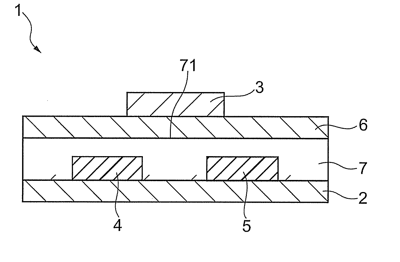
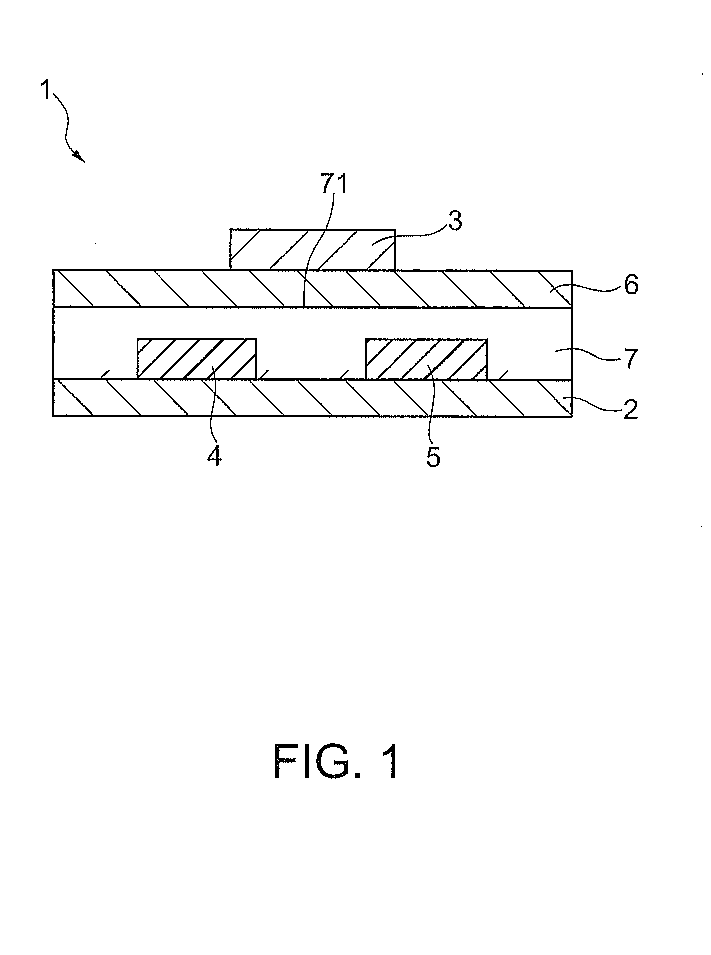
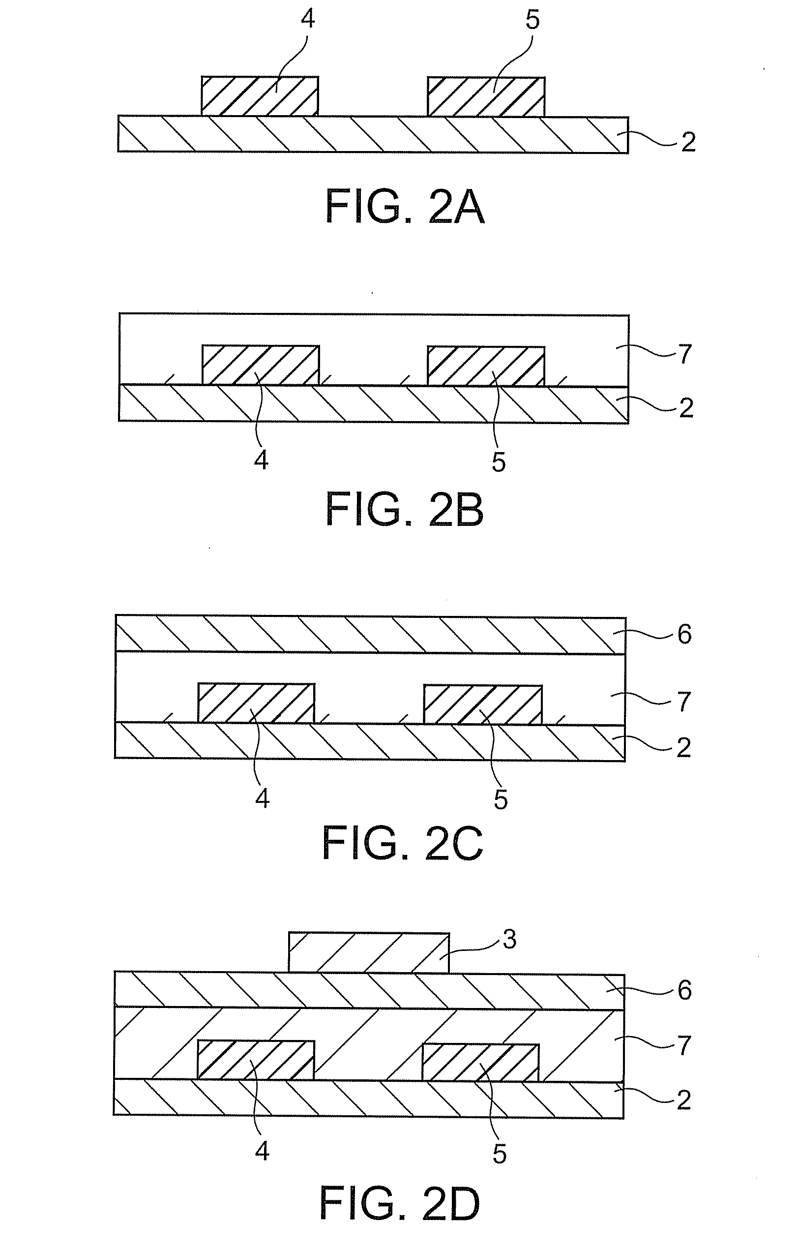
[0061]FIG. 1 is a longitudinal sectional view schematically showing a semiconductor device of the first embodiment, while FIGS. 2A through 2D are diagrams (longitudinal sectional views) for explaining a method for manufacturing the semiconductor device shown in FIG. 1.

[0062]In the following description, the upper side in FIGS. 1 through 2D is described as “top”, while the lower side is described as “bottom”.

[0063]In a semiconductor device 1 shown in FIG. 1, a source electrode 4 and a drain electrode 5 are formed on a top surface of a substrate 2 so as to be apart from each other, and an organic semiconductor layer 7 is formed so as to cover them. On a top surface of the organic semiconductor layer 7, a gate insulation layer 6 is formed. Further, a gate electrode 3 is formed on a top surface of the gate insulation layer 6. That is, the semiconductor device 1 shown in FIG. 1 has a top gate bottom con...

second embodiment

[0161]Next, a second embodiment of the semiconductor device will be described.

[0162]FIG. 3 is a sectional view schematically showing a semiconductor device of the second embodiment, while FIGS. 4A through 4D are diagrams (longitudinal sectional views) for explaining a method for manufacturing the semiconductor device shown in FIG. 3.

[0163]In the following description, the upper side in FIGS. 3 through 4D is described as “top”, while the lower side is described as “bottom”.

[0164]The following description of the second embodiment of the semiconductor device focuses primarily on differences from the first embodiment, and similar points will be omitted.

[0165]The semiconductor device 1 of the second embodiment is different in the overall configuration from the semiconductor device 1 of the first embodiment and is the same in other sections.

[0166]In the semiconductor device 1 shown in FIG. 3, the gate electrode 3 is formed on the top surface of the substrate 2. On the substrate 2, the gat...

example 1

[0229][1] Source Electrode and Drain Electrode Forming Step

[0230]First, a plastic substrate was prepared and cleaned with ethanol so as to degrease its surface.

[0231]A source electrode and a drain electrode were formed on the plastic substrate by depositing gold. After the source electrode and the drain electrode were formed, the plastic substrate having the source electrode and the drain electrode formed thereon was immersed in isopropyl alcohol and subjected to an ultrasonic cleaning for 5 minutes. After the cleaning, the plastic substrate was dried at 60 degrees Celsius for 10 minutes.

[0232][2] Organic Semiconductor Layer Forming Step

[0233]Next, fluorene-bithiophene copolymer (American Dye Source-made F8T2, hereinafter, abbreviated as “F8T2”) was dissolved in toluene so as to prepare a 0.5 wt % F8T2 solution. The F8T2 solution was supplied on the source electrode, the drain electrode, and the substrate by spin casting so as to form a F8T2 film having a thickness of 20 nm as a lay...


PUM

PropertyMeasurementUnit
water absorptionaaaaaaaaaa
boiling pointaaaaaaaaaa
thicknessaaaaaaaaaa

Abstract

A method for manufacturing a semiconductor device includes: forming a source electrode and a drain electrode on a substrate; forming an organic semiconductor layer including a π conjugated organic compound at least between the source electrode and the drain electrode; applying an application liquid on the organic semiconductor layer, the application liquid being made of a polymer of an alicyclic compound dissolved in a paraffin hydrocarbon solvent that is a carbocyclic compound without having aromaticity; forming a gate insulation layer including the polymer of the alicyclic compound by removing the paraffin hydrocarbon solvent from the application liquid; and forming a gate electrode on the gate insulation layer.

Description

[0001]The entire disclosure of Japanese Patent Application No. 2007-086099, filed Mar. 28, 2007 is expressly incorporated by reference herein.BACKGROUND[0002]1. Technical Field[0003]The present invention relates to a method for manufacturing a semiconductor device, the semiconductor device, a semiconductor circuit, an electro-optical device, and an electronic apparatus.[0004]2. Related Art[0005]In recent years, researches on an organic device become more and more active because it is anticipated to be light weight, flexible, and at a low cost. In particular, an organic thin film transistor (hereinafter, abbreviated as “TFT”) is increasingly expected to be applied to electric papers, wireless tags, plastic IC cards, and further, in fields of medical application such as biosensors for practical use.[0006]As a process for manufacturing an organic TFT, vacuum processing such as vapor deposition, and a coating process such as spin coating and an inkjet method are applicable.[0007]Since s...

Claims


Application Information

Patent Timeline
Patent Type & Authority Applications(United States)
IPC IPC(8): H01L51/10H01L51/40
CPCH01L51/0007H01L51/0036H01L51/0039H01L51/0043H01L51/052H01L51/0541H01L51/0545H10K71/15H10K85/115H10K85/113H10K85/151H10K10/471H10K10/464H10K10/466
Inventor MASUDA, TAKASHI
Owner E INK CORPORATION
Why Eureka
Try Eureka