Magneto-resistance effect element, and method for manufacturing the same

Active Publication Date: 2008-10-02
TDK CORPARATION +1
View PDF54 Cites 29 Cited by
  • Summary
  • Abstract
  • Description
  • Claims
  • Application Information

AI Technical Summary

Benefits of technology

[0015]An aspect of the present invention relates to a magneto-resistance effect element, comprising: a fixed magnetization layer of which a magnetization is substantially fixed in one direction; a free magnetization layer of which a magnetization is rotated in accordance with an external magnetic field and which is formed opposite to the fixed magnetization layer; a spacer layer including a current confining layer with an insulating layer and a conductor to pass a current through the i

Problems solved by technology

Herein, a metal CPP-GMR element of which the spin valve film is made of a metallic layer ha

Method used


Image

  • Magneto-resistance effect element, and method for manufacturing the same
  • Magneto-resistance effect element, and method for manufacturing the same
  • Magneto-resistance effect element, and method for manufacturing the same

Examples


example 1

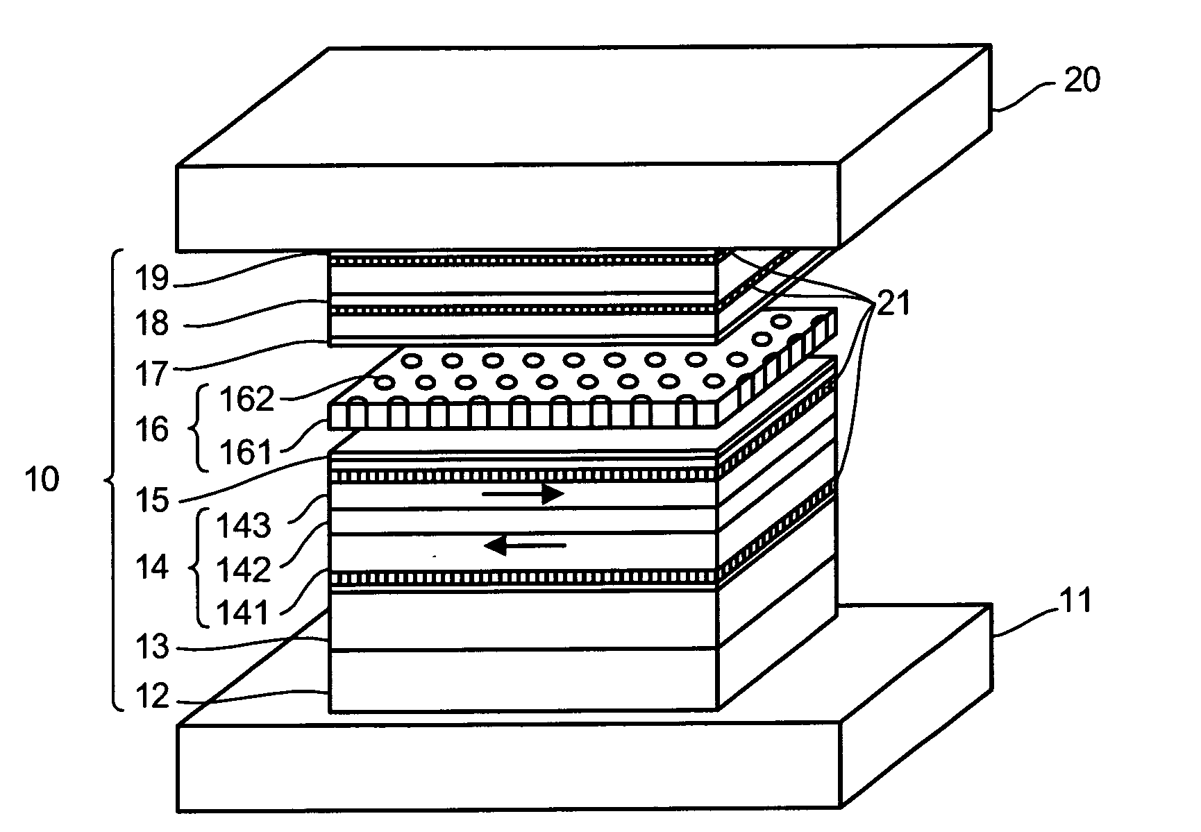
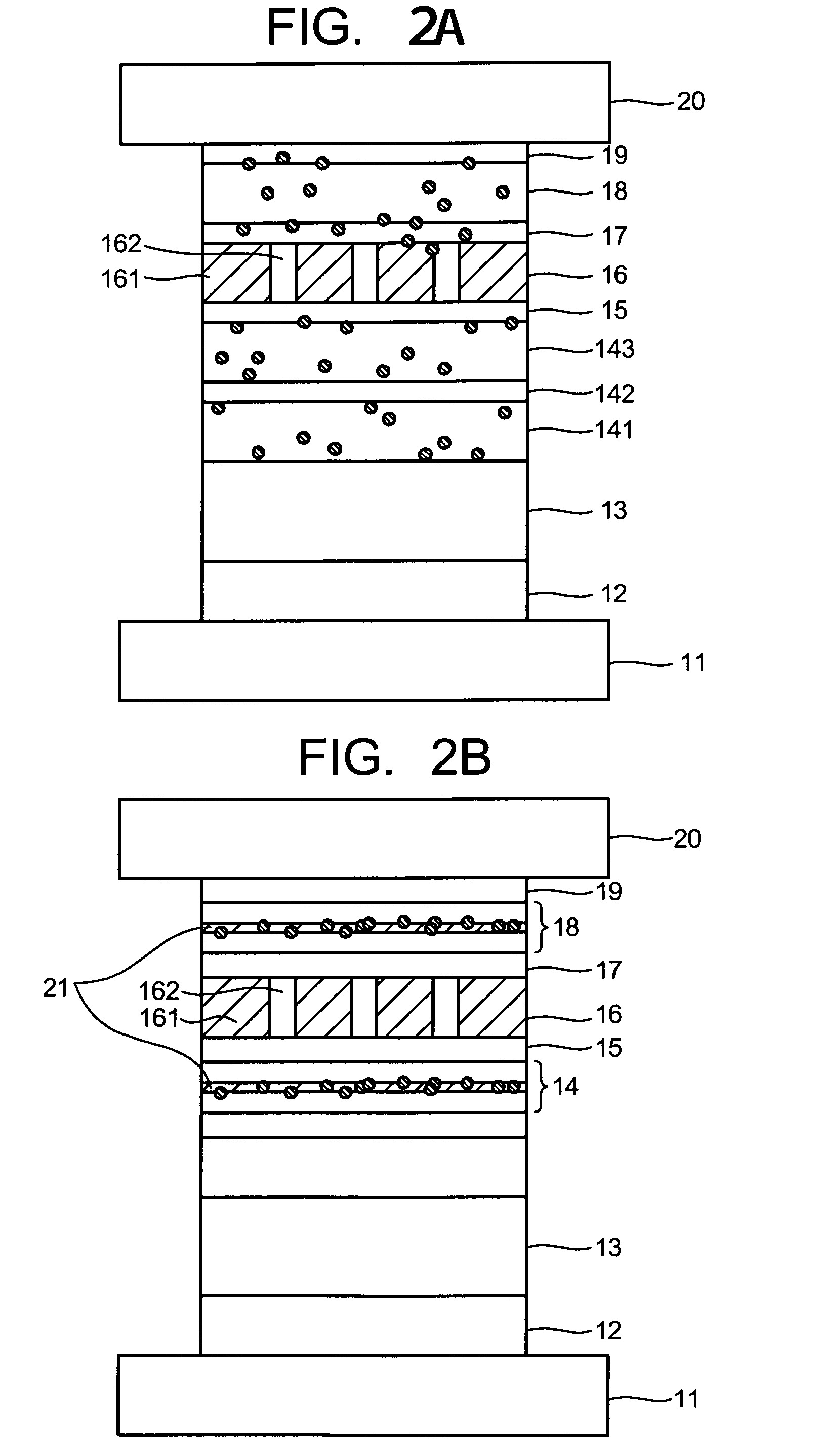
[0156]In this embodiment, the film structure was configured below.

Bottom electrode 11Underlayer 12Ta 5 nm / Ru 2 nmPinning layer 13Ir22Mn78 7 nmPinned layer 14Co75Fe25 3.3 nm / Ru 0.9 nm / Fe50Co50 1 nm / Cu 0.25 nm × 2 / Fe50Co501 nmMetallic layer 15Cu 0.6 nmCurrent confining layer 16insulating layer 161 ofAl2O3 and current confining path 162 of CuMetallic layer 17Cu 0.4 nmFree layer 18described laterCap layer 19Cu 1 nm / Ta 2 nm / Ru 15 nmTop electrode 20

[0157]In this embodiment, the characteristics of the magneto-resistance effect element was investigated with and without the functional layer in the free layer 18. Example 1 corresponds to the magneto-resistance effect element with the functional layer and Comparative Example 1 corresponds to the magneto-resistance effect element without the functional layer. The results are listed in Table 2.

TABLE 2MRvariationFree layer 18ratio [%]Example 1Co60Fe40 [2 nm] / functional layer Si [0.25 nm] / 10.5Ni83Fe17 [3.5 nm]ComparativeCo60Fe40 [2 nm] / Ni83Fe17 [3...

example 2

[0159]In this embodiment, the functional layer was formed at various positions of the free layer 18 and the cap layer 19. The fundamental film structure will be listed below.

Bottom electrode 11Underlayer 12Ta 5 nm / Ru 2 nmPinning layer 13Ir22Mn78 7 nmPinned layer 14Co75Fe25 3.9 nm / Ru 0.9 nm / Fe50Co50 1.8 nm / Cu 0.25 nm / Fe50Co501.8 nmMetallic layer 15Cu 0.6 nmCurrent confining layer 16insulating layer 161 ofAl2O3 and current confining path 162 of CuMetallic layer 17Cu 0.4 nmFree layer 18described laterCap layer 19described laterTop electrode 20

[0160]The thickness of the pinned layer 14 of the film structure in Example 2 is larger than the thickness of the pinned layer 14 of the film structure in Example 1. If the thickness of the pinned layer 14 is set larger, the crystallinity of the top pinned layer 143 is enhanced so as to enhance the MR through the enhancement of the spin dependent bulk scattering effect. The film structure of the free layer 18 and the cap layer 19 will be listed in...

example 3

[0162]In this embodiment, the functional layers were formed in the pinned layer 14 and the free layer 18. The fundamental film structure will be listed below.

Bottom electrode 11Underlayer 12Ta 5 nm / Ru 2 nmPinning layer 13Ir22Mn78 7 nmPinned layer 14described laterMetallic layer 15Cu 0.6 nmCurrent confining layer 16insulating layer 161 ofAl2O3 and current confining path 162 of CuMetallic layer 17Cu 0.4 nmFree layer 18described laterCap layer 19Cu 1 nm / Ta 2 nm / Ru 15 nmTop electrode 20

[0163]The film structure of the pinned layer 14 and the free layer 18 will be listed in Table 4. In Example 3, the Si functional layer is formed in the top pinned layer 143, which is different from Example 2. The results are listed in Table 4.

TABLE 4MRvariationPinned layer 14Free layer 14ratio [%]Example 3Co75Fe25 [3.9 nm] / RuCo60Fe40 [2 nm] / 12.8[0.9 nm] / Fe50Co50 [0.6 nm] / functional layer Si [0.25 nm] / functional layer Si [0.25 nm] / Ni83Fe17 [3.5 nm]Fe50Co50 [1.2 nm] / Cu[0.25 nm] / Fe50Co50 [1.8 nm]Example 2ACo...


PUM


Abstract

A magneto-resistance effect element, including:
a fixed magnetization layer of which a magnetization is substantially fixed in one direction; a free magnetization layer of which a magnetization is rotated in accordance with an external magnetic field and which is formed opposite to the fixed magnetization layer; a spacer layer including a current confining layer with an insulating layer and a conductor to pass a current through the insulating layer in a thickness direction thereof and which is located between the fixed magnetization layer and the free magnetization layer; a thin film layer which is located in a side opposite to the spacer layer relative to the free magnetization layer; and a functional layer containing at least one element selected from the group consisting of Si, Mg, B, Al which is formed in or on at least one of the fixed magnetization layer, the free magnetization layer and the thin film layer.

Description

CROSS-REFERENCE TO RELATED APPLICATIONS[0001]This application is based upon and claims the benefit of priority from the prior Japanese Patent Application No. 2007-094474, filed on Mar. 30, 2007; the entire contents of which are incorporated herein by reference.BACKGROUND OF THE INVENTION[0002]1. Field of the Invention[0003]The present invention relates to a magneto-resistance effect element which is configured such that a current is flowed in the direction perpendicular to the film surface thereof to detect the magnetization of the element and the magneto-resistance effect element and to a method for manufacturing the same.[0004]2. Description of the Related Art[0005]Recently, the miniaturization and the high density recording of a hard disk drive (HDD) is remarkably required and being progressed. In the future, it is promised to much develop the high density recording of the HDD. The HDD of high density recording can be realized by narrowing the recording track width. However, the ...

Claims


Application Information

Patent Timeline
IPC IPC(8): G11B5/33
CPCB82Y10/00B82Y25/00G01R33/093G11B5/3906G11B5/3909G11B2005/3996H01L43/08G11B5/39Y10S977/943H10N50/10
Inventor FUJI, YOSHIHIKOFUKUZAMA, HIDEAKIYUASA, HIROMIZHANG, KUNLIANGLI, MINHARA, MICHIKOKUROSAKI, YOSHINARI
Owner TDK CORPARATION
Why Eureka
Try Eureka