Control of ion angular distribution function at wafer surface

Inactive Publication Date: 2008-10-02
TOKYO ELECTRON LTD
View PDF3 Cites 40 Cited by
  • Summary
  • Abstract
  • Description
  • Claims
  • Application Information

AI Technical Summary

Benefits of technology

[0011]An objective of the present invention is to provide a method and apparatus for controlling the IADF at a wafer surface during plasma processing. A particular objective of the invention is to provide IADF-controlled plasma processing, and particularly IADF control that is independent of wafer holder RF bias power and frequency and of operating pressure.
[0012]One objective of the invention is to control the IADF at one or more given points on the surface of a wafer, for example, to deliver ions to sidewall surfaces of features on a wafer. A further objective of the invention is to control the variation of IADF across the surface of a wafer, either to vary the IADF function across the wafer surface or to make the IADF uniform across the wafer surface, for example, to compensate for the effects of conditions that would undesirably affect IADF.

Problems solved by technology

Control of IADF to produce ideal feature coverage has been a challenge in the prior art.

Method used


Image

  • Control of ion angular distribution function at wafer surface
  • Control of ion angular distribution function at wafer surface
  • Control of ion angular distribution function at wafer surface

Examples


Embodiment Construction

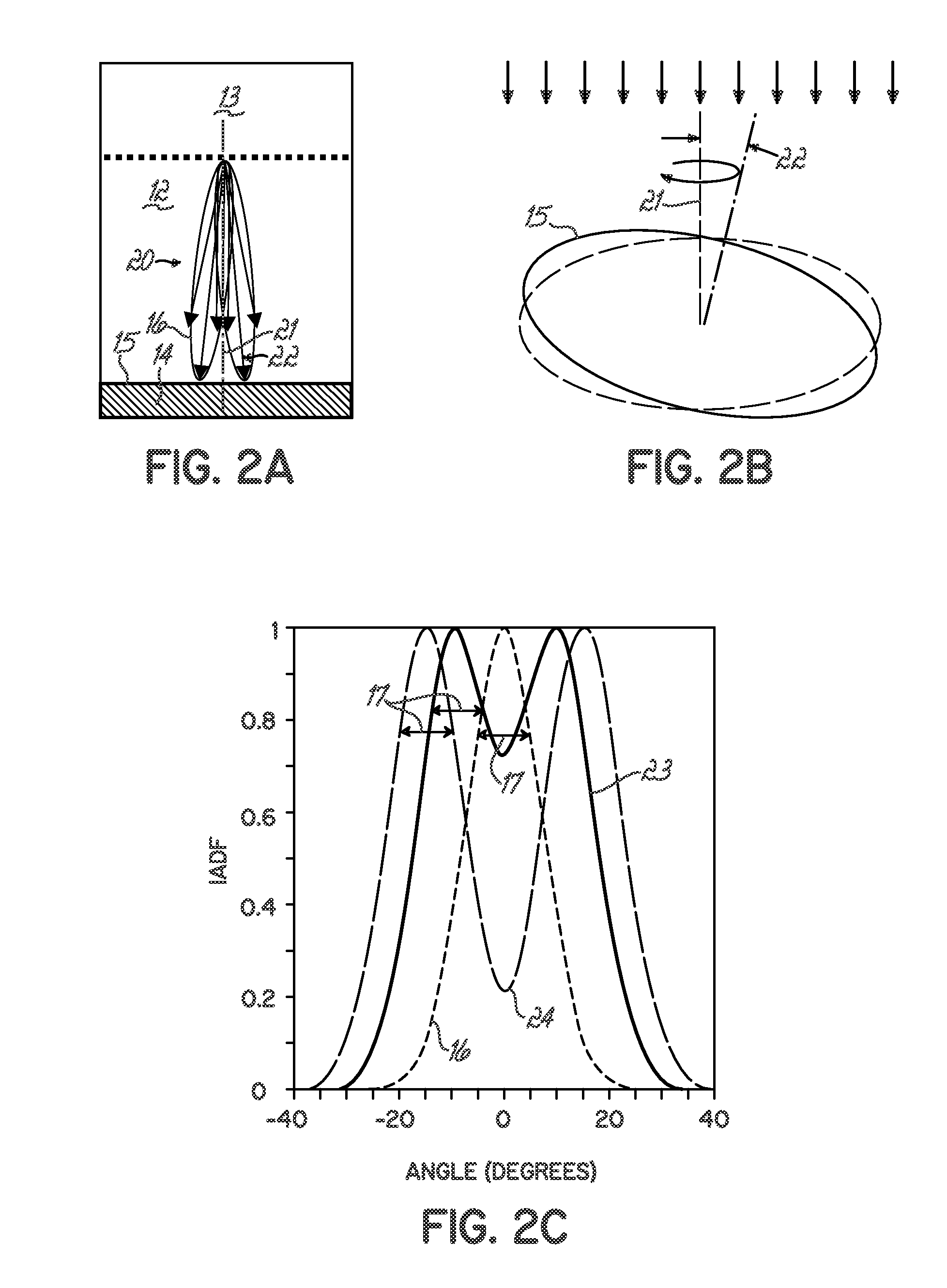
[0036]An example of an ion angular distribution function (IADF) 20 produced by the present invention that creates increased sidewall coverage of features in ionized physical vapor distribution (IPVD) is shown in cross-section in FIG. 2A under conditions typical for IPVD. The IADF 20 is not typical of current prior art plasma processing. Mathematically, the IADF 20 can be described as a rotation of the natural IADF 16 (FIG. 1A) at certain angle 22 around an axis 21 that is perpendicular to the surface of the substrate 15, as illustrated in FIG. 2B. One such IADF 20 might, for example, be that produced in a vacuum process in which a well-collimated ion beam impinges along the axis 21 on the surface of a wafer 15 that is inclined at the angle 22 to the axis 21 and is rotating around the axis 21, where the process occurs in high vacuum to yield a very low dispersion of the ion beam. The IADF 20, so produced, is compared to the IADF 16 by curves 23 and 24 in FIG. 2C, in which IADF 20 is ...


PUM

PropertyMeasurementUnit
electric fieldaaaaaaaaaa
pressuresaaaaaaaaaa
pressuresaaaaaaaaaa

Abstract

A manufacturing method and apparatus for IC fabrication controls the ion angular distribution at the surface of a wafer with electrodes in a wafer support that produce electric fields parallel to the wafer surface without disturbing plasma parameters beyond the wafer surface. The ion angular distribution function (IADF) at the wafer surface is controlled for better feature coverage or etching. Grid structure is built into the substrate holder within the coating at the top of the holder. The grid components are electrically biased to provide electric fields that combine with the sheath field to distribute the ion incidence angles from the plasma sheath onto the wafer. The grid can be dynamically biased or phased to control uniformity of the effects.

Description

[0001]The present invention relates to integrated circuit (IC) fabrication and to the control of the ions onto the surface of a wafer during processing. More particularly, the invention relates the control of the angles of incidence of ions onto a wafer surface during plasma processing of a semiconductor wafer held on RF-biased wafer holders in processing tools for thin film material processing.BACKGROUND OF THE INVENTION[0002]In plasma processing systems, semiconductor wafers are placed on the RF biased substrate holders, such as electrostatic chucks (ESCs) or chucks provided with mechanical wafer clamps, where the wafers are exposed to ions from the plasma. The energy of the ions incident on the wafers from the plasma is typically independently controlled by varying the bias power level, while the ion density is usually controlled by control of an independent plasma source. The plasma source can be, for example, an inductively coupled plasma (ICP) source, a dual capacitively-coupl...

Claims


Application Information

Patent Timeline
Patent Type & Authority Applications(United States)
IPC IPC(8): H01L21/265G21K5/00
CPCH01J37/32623H01J37/32706
Inventor BRCKA, JOZEF
Owner TOKYO ELECTRON LTD
Why Eureka
Try Eureka