Method for designing mask pattern and method for manufacturing semiconductor device

a mask pattern and semiconductor technology, applied in the field of manufacturing technology of semiconductor devices, can solve the problems of increasing the cost of advance preparation and the large storage area required, and achieve the effects of increasing the processing time of opc, increasing the processing cost, and increasing the processing tim

Inactive Publication Date: 2008-10-09
RENESAS TECH CORP +1
View PDF3 Cites 24 Cited by
  • Summary
  • Abstract
  • Description
  • Claims
  • Application Information

AI Technical Summary

Benefits of technology

[0032]Increase of the OPC processing time deteriorates a manufacture TAT (Turn Around Time) of a semiconductor device including a mask pattern generation, and it also causes increase in cost.
[0033]In view of these circumstances, an object of the present invention is to provide a mask pattern designing technology comprising an OPC process which can achieve the reduction in an increasing OPC processing time, reduce a manufacture TAT for a semiconductor device, and reduce the cost.
[0034]Another object of the present invention is to provide a manufacturing technology of an electronic circuit device and a semiconductor device capable of generating the mask pattern within a practical time period to reduce a manufacturing period.

Problems solved by technology

Therefore, such a problem arises that cost required for advance preparation increases and much storage region is required.

Method used


Image

  • Method for designing mask pattern and method for manufacturing semiconductor device
  • Method for designing mask pattern and method for manufacturing semiconductor device
  • Method for designing mask pattern and method for manufacturing semiconductor device

Examples


first embodiment

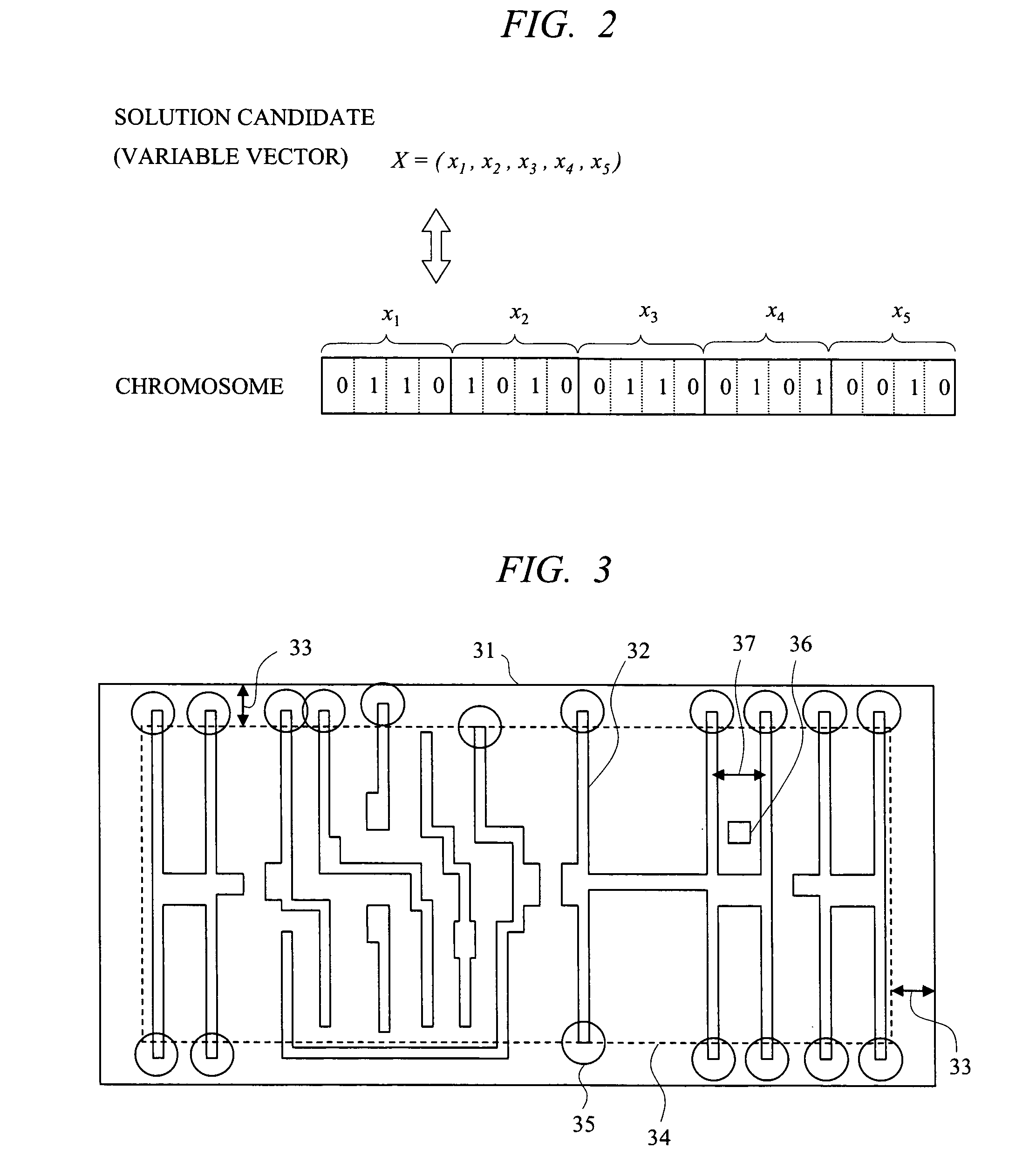
[0056]The mask pattern designing method according to a first embodiment of the present invention is performed using a computer or the like. The first embodiment of the present invention will be described with reference to FIG. 3. FIG. 3 shows an example where a pattern 32 is arranged in a standard cell.

[0057]As shown in FIG. 3, most of the end portions of the pattern 32 are located near a cell boundary 31, and the patterns of the end portions are deformed due to the influence from the cells arranged around them. Meanwhile, since the influence of the optical proximity effect is reduced for the patterns inside a distance 33 from the cell boundary 31, the influence from the cell patterns arranged around them is small. The layer of the pattern 32 is not particularly defined. However, it has been found out as a result of various examinations that the distance 33 where the influence reaches is 0.85 P on the basis of the minimum pattern pitch (P) 37 interposing a contact hole 36 in the cas...

second embodiment

[0060]A second embodiment of the present invention will be described with reference to FIG. 4 to FIG. 7. FIG. 4 shows an example of a standard cell, in which a reference numeral 44 denotes a cell boundary. A reference numeral 41 denotes a gate wire, 42 denotes a diffusion layer, and 43 denotes a contact hole. Similar to the first embodiment, most of end portions of the gate wire are located near the cell boundary.

[0061]A gate length 49 requires the highest dimensional accuracy in a gate, but it is hardly influenced by the proximity effects of the other cells and patterns arranged around the cell other than a gate pattern 41b which is located near the periphery portion. This is because of the long distance from the external patterns and because the patterns which are arranged above and below the gate extending in a longitudinal direction and the gate length which is a width in a lateral direction are in the positional relationship where the interaction therebetween hardly occurs. The...

third embodiment

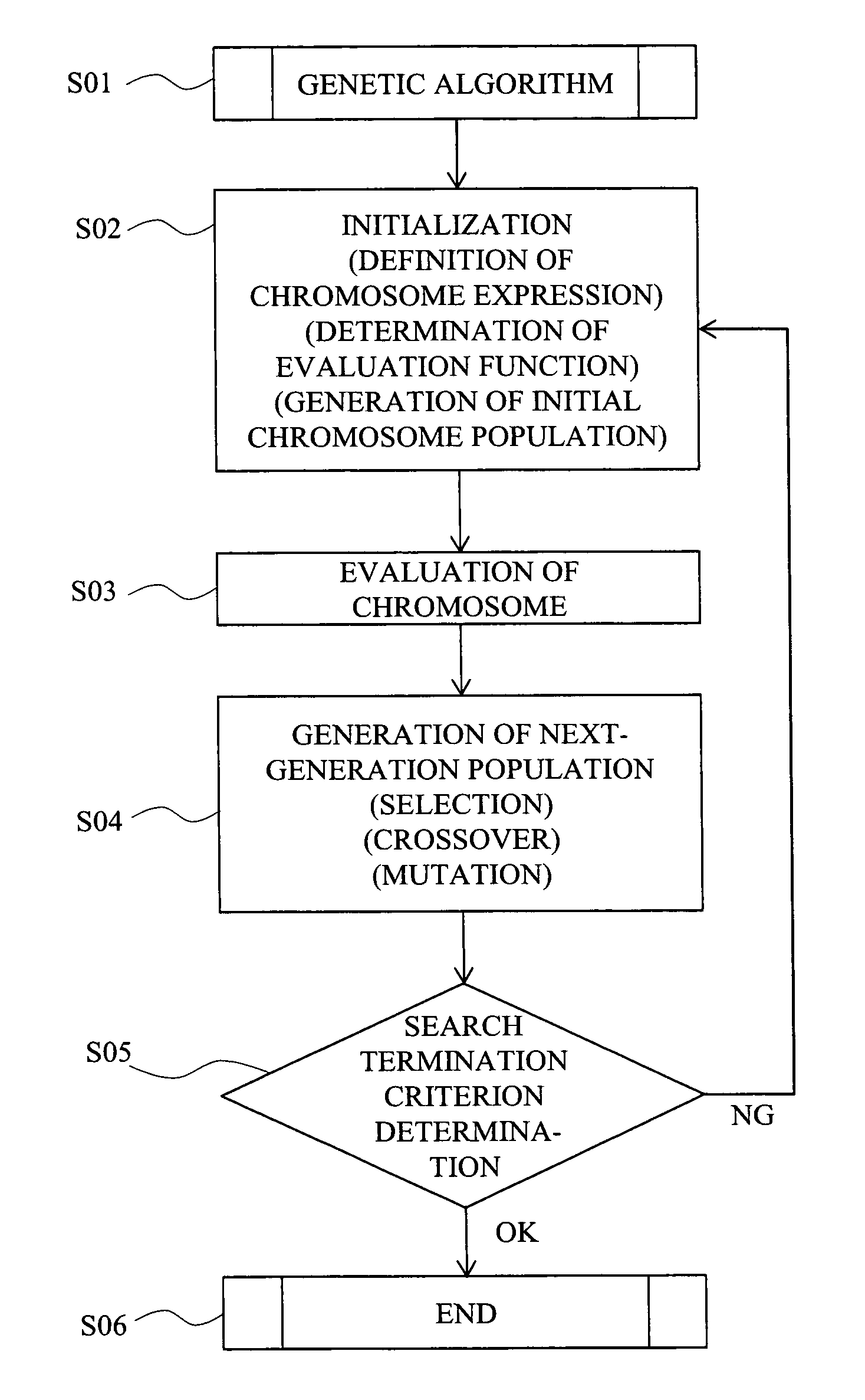
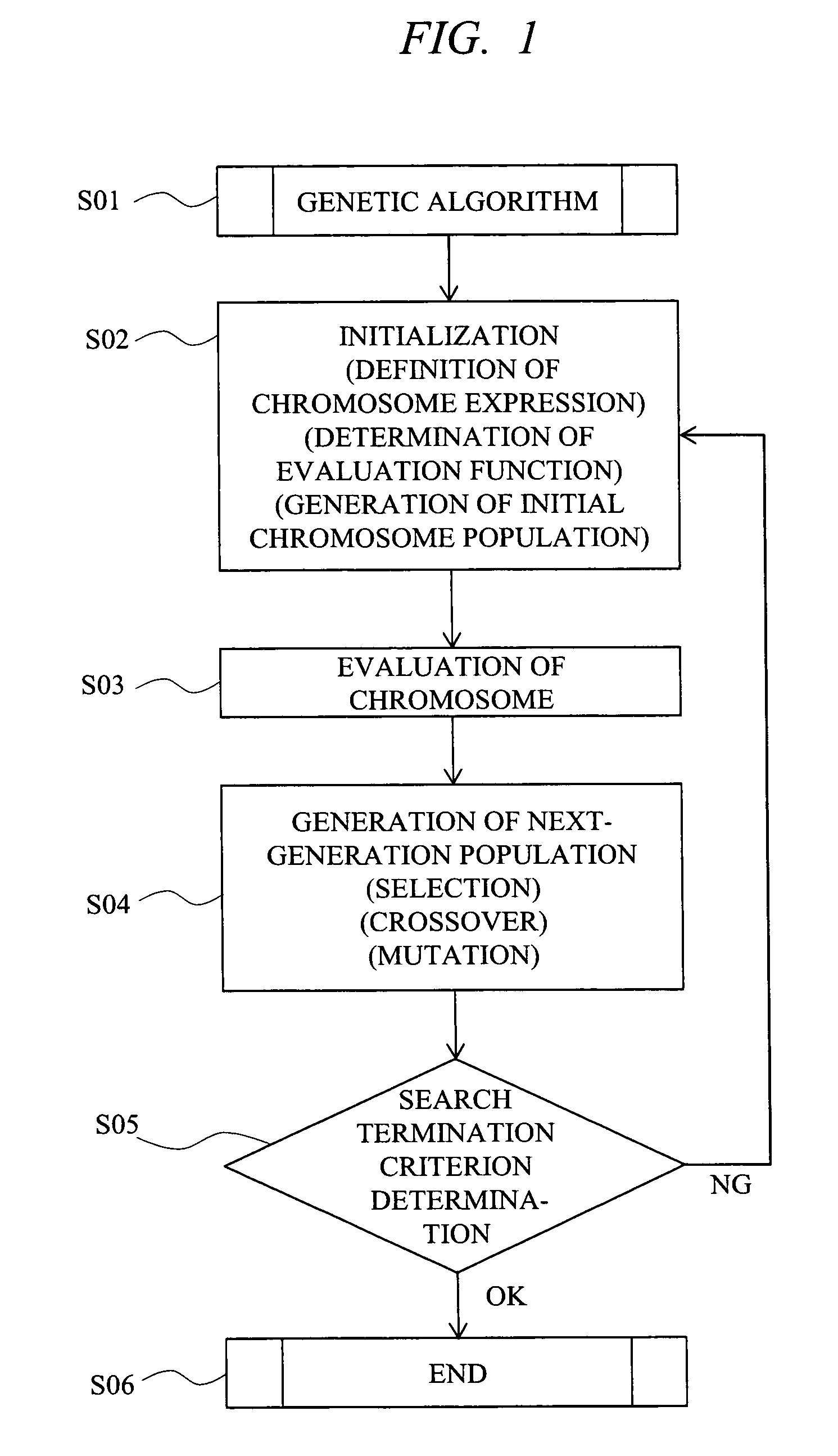
[0066]In this embodiment, an example of the re-correction by OPC for a pattern end portion by using the genetic algorithm will be described based on the correction for a hammer head shape.

[0067]An application method of the genetic algorithm will be described below. Since a calculation procedure of the genetic algorithm is the same as that described in the “Summary of the Invention”, details of respective steps will be described here.

[Initialization: Definition of Chromosome Expression]

[0068]In the third embodiment, each variable is handled as a real number directly indicating a size of a figure. That is, respective elements xi (i=1, 2, . . . , 8) in the variable vector X are expressed using real numbers, and they correspond to pi (i=1, 2, . . . , 8) in FIG. 8. At this time, it is possible to adopt a difference from a design target as a chromosome expression instead of a value of the size itself. Alternatively, instead of representing respective elements xi in the variable vector X u...


PUM

PropertyMeasurementUnit
gate widthaaaaaaaaaa
timeaaaaaaaaaa

Abstract

A mask pattern designing method capable of achieving the reduction in the increasing OPC processing time, shortening the manufacture TAT of a semiconductor device, and achieving the cost reduction is provided. An OPC (optical proximity correction) process at the time when a cell is singularly arranged is performed to a cell library pattern which forms a basic structure of a semiconductor circuit pattern in advance, and a semiconductor chip is produced using the cell library pattern to which the OPC process has been performed. At this time, since the cell library pattern which has been OPC-processed in advance is influenced by the cell library patterns around it, the correction process thereof is performed to the end portions of the patterns near the cell boundary. As particularly effective OPC correction means, the genetic algorithm is used.

Description

CROSS-REFERENCE TO RELATED APPLICATION[0001]The present application claims priority from Japanese Patent Application No. JP 2005-277331 filed on Sep. 26, 2005, the content of which is hereby incorporated by reference into this application.TECHNICAL FIELD OF THE INVENTION[0002]The present invention relates to a manufacturing technology of a semiconductor device. In particular, it relates to a technology effectively applied to a mask pattern designing process for forming a pattern smaller than an exposure wavelength in optical lithography.BACKGROUND OF THE INVENTION[0003]Semiconductor devices can be mass-produced by repeating photolithography steps of irradiating exposure light to a mask which is a master plate in which a circuit pattern is written to transfer the pattern onto a semiconductor substrate (hereinafter, referred to as wafer) via a reduction optical system. In recent years, it has been required to form a pattern having a dimension smaller than an exposure wavelength in opt...

Claims


Application Information

Patent Timeline
Patent Type & Authority Applications(United States)
IPC IPC(8): G06F17/50G03F1/36G03F1/68
CPCG03F1/144G03F1/36G06F17/5081G06F2217/08G06F2111/06G06F30/398
Inventor TANAKA, TOSHIHIKOTERASAWA, TSUNEOYOSHIOKA, NOBUYUKIHIGUCHI, TETSUYASAKANASHI, HIDENORINOSATO, HIROKAZUMURAKAWA, MASAHIRO
Owner RENESAS TECH CORP
Why Eureka
Try Eureka