

Fabrication of Electrically Active Films Based on Multiple Layers
- Summary
- Abstract
- Description
- Claims
- Application Information
AI Technical Summary
Benefits of technology
Problems solved by technology
Method used
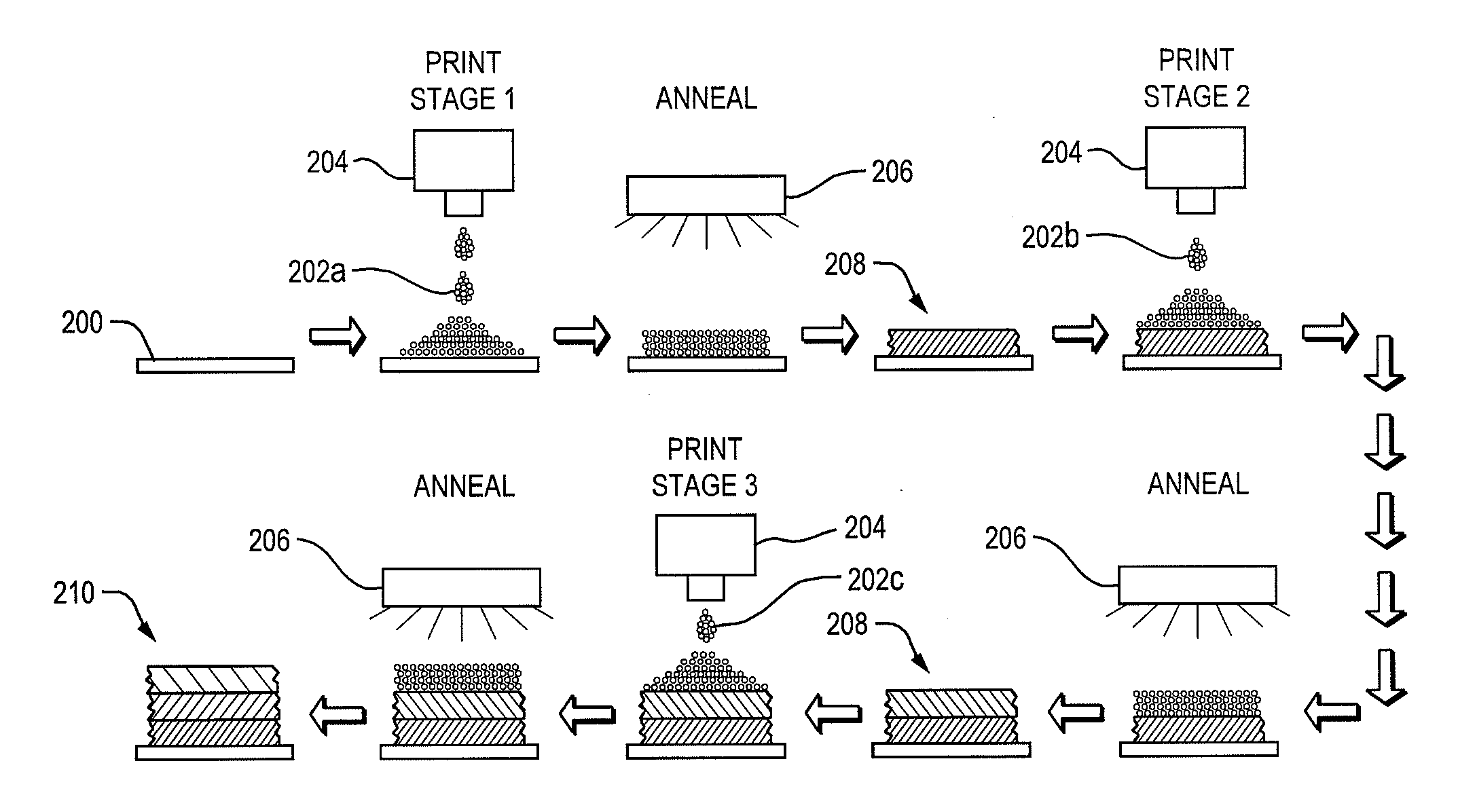
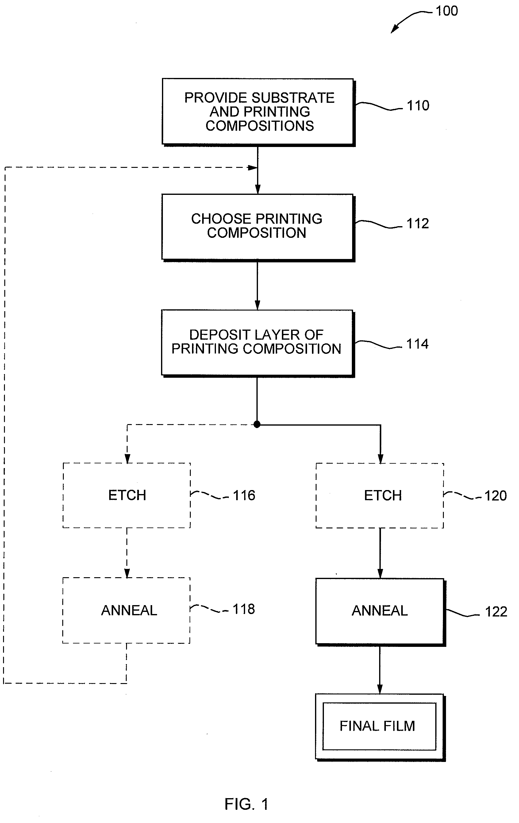
Image

Examples
example 1
[0030]Cu(I) acetate (1 mmol) and In(III) acetate (1 mmol) are added to a clean and dry RB-flask. Octadecene ODE (5 mL) is added the reaction mixture heated at 100° C. under vacuum for 30 mins. The flask is back-filled with nitrogen and the temperature raised to 140° C. 1-octane selenol is injected and the temperature falls to 120° C. The resulting orange suspension is heated with stirring and a transparent orange / red solution is obtained when the temperature has reached 140° C. This temperature is maintained for 30 minutes, then IM tri-octyl-phoshine selenide TOPSe (2 mL, 2 mmol) is added dropwise and the solution heated at 160° C. The PL is monitored until it reaches the desired wavelength, after which it is cooled and the resulting oil washed with methanol / acetone (2:1) 4-5 times and finally isolated by precipitation with acetone.
example 2
Large Scale Production
[0031]A stock solution of TOPSe was prepared by dissolving Se powder (10.9, 138 mmol) in TOP (60 mL) under nitrogen. To dry, degassed ODE was added Cu(I) acetate (7.89 g, 64.4 mmol) and In(III) acetate (20.0 g, 68.5 mmol). The reaction vessel was evacuated and heated at 140° C. for 10 min, backfilled with N2 and cooled to room temp. 1-Octane selenol (200 mL) was added to produce a bright orange suspension. The temperature of the flask was raised to 140° C. and acetic acid distilled from the reaction at 120° C. On reaching 140° C. the TOPSe solution was added dropwise over the course of 1 hour. After 3 hours the temperature was raised to 160° C. The progress of the reaction was monitored by taking aliquots from the reaction periodically and measuring the UV / Visible and photoluminescence spectra. After 7 hours the reaction was cooled to room temperature and the resulting black oil washed with methanol. Methanol washing was continued until it was possible to preci...
PUM
| Property | Measurement | Unit |
|---|---|---|
| Thickness | aaaaa | aaaaa |
| Size | aaaaa | aaaaa |
| Nanoscale particle size | aaaaa | aaaaa |
Abstract
Description
Claims
Application Information