Method of forming a pattern in a semiconductor device and method of forming a gate using the same

a technology of semiconductor devices and patterns, which is applied in the direction of instruments, photomechanical devices, optics, etc., can solve the problems of gate size reduction, uneven thickness of the etched portion of the thin layer, and uneven thickness of the etched portion, so as to reduce the roughness of the line edge due to the photolithography process, the effect of small line width and small deviation of line width

Active Publication Date: 2008-10-23
SAMSUNG ELECTRONICS CO LTD
View PDF7 Cites 10 Cited by
  • Summary
  • Abstract
  • Description
  • Claims
  • Application Information

AI Technical Summary

Benefits of technology

[0018]Since the cell hard mask pattern is formed on sidewalls of the buffer pattern, a pair of patterns is repeatedly formed at regular intervals in the cell region. That is, the present invention may be applied to a method of manufacturing the semiconductor device in which a pair of patterns is repeated at regular intervals in the cell region. In addition, since the peripheral hard mask pattern is always formed without a limitation in its shape, the minute pattern in the peripheral region is readily formed in accordance with various design conditions.
[0020]Therefore, the pattern in the wafer may have a different line width according to the region of the wafer, and the line width may be less than the CD of the photolithography process. In addition, the line width variation due to the photolithography process may be minimized. Further, since the hard mask layer is uniformly etched away, line edge roughness due to a non-uniform etching may also be minimized.
[0027]Therefore, the gate pattern formed to have a smaller line width in the cell region than in the peripheral region. In addition, the line width variation and the line edge roughness due to the photolithography process may be minimized.

Problems solved by technology

Thirdly, when an etching process is performed using the photoresist pattern as a mask, an edge line of an etched portion of the thin layer becomes very rough since the photoresist pattern becomes non-uniform, which is referred to as a line edge roughness phenomenon.
Non-uniformity of the line width distribution causes electrical characteristics of each unit device in a chip or in a wafer to be non-uniform, thus causing various process failures in the semiconductor device.
In addition, a non-uniform etching of the photoresist film degrades a short channel characteristic of the device, and a gate size reduction accelerates the degradation of the short channel characteristic of the device.
However, when the second insulating layer is used as an etching mask, the pattern has the same line width across a whole surface of a substrate, and as a result, the pattern may not have a line width greater than that of the second insulating layer at any local area on the substrate.

Method used


Image

  • Method of forming a pattern in a semiconductor device and method of forming a gate using the same
  • Method of forming a pattern in a semiconductor device and method of forming a gate using the same
  • Method of forming a pattern in a semiconductor device and method of forming a gate using the same

Examples


embodiment 1

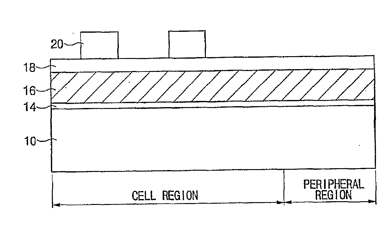
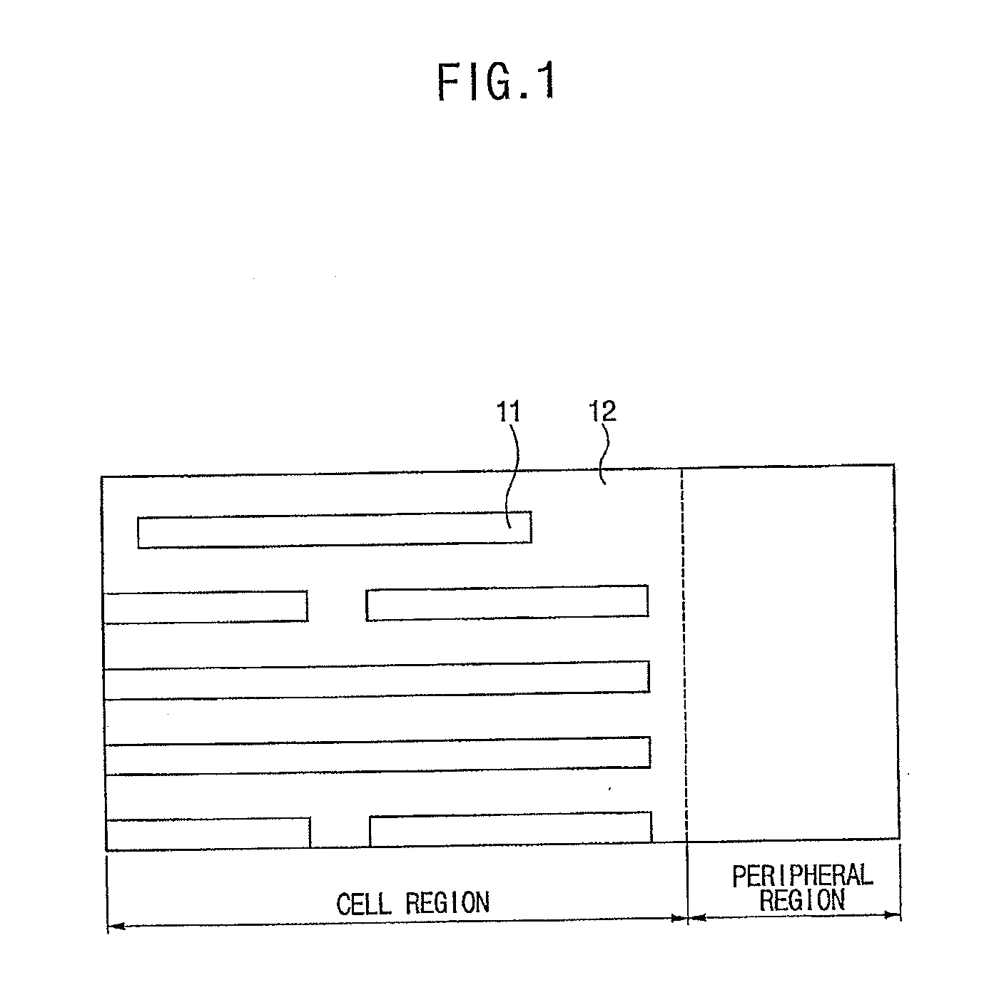
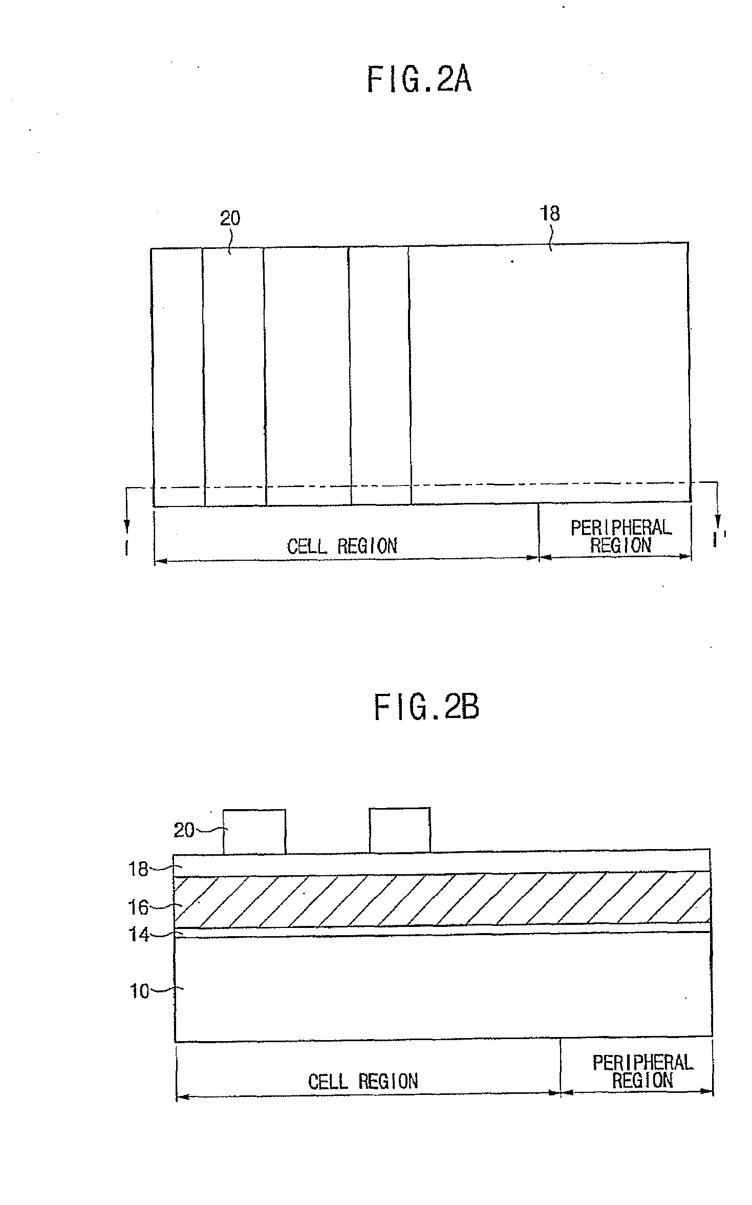
[0041]FIG. 1 is a plan view illustrating a semiconductor substrate that is divided into a cell region and a peripheral region. FIGS. 2A through 8B are plan views and cross sectional views showing processing steps of a method of forming a pattern of an I-type static random access memory (SRAM) device according to a first embodiment of the present invention. Throughout FIGS. 2A through 8B, each capital letter A designates a plan view illustrating the I-type SRAM device, and each capital letter B designates a cross sectional view taken along the line I-I′ of the corresponding figure designated by the capital letter A.

[0042]Referring to FIG. 1, a semiconductor substrate including a cell region and a peripheral region is provided. A unit memory device is positioned in the cell region, and a driving circuit for driving the unit memory device is positioned in the peripheral region. A plurality of N type impurities is selectively supplied to surface portions of the silicon substrate at whic...

embodiment 2

[0061]FIGS. 9A through 11 are plan views and cross sectional views showing processing steps of a method of forming a pattern of an I-type static random access memory (SRAM) device according to a second embodiment of the present invention. Throughout FIGS. 9A through 10B, each capital letter A designates a plan view illustrating the I-type SRAM device, and each capital letter B designates a cross sectional view taken along the line I-I′ of the corresponding figure designated by the capital letter A.

[0062]The present second embodiment of the present invention is the same as the first embodiment of the present invention except that a separation layer is added between the gate electrode layer and the buffer layer.

[0063]Referring to FIGS. 9A and 9B, a semiconductor substrate 10 including a cell region and a peripheral region is provided, and a field region and an active region are defined by the same process as described in the first embodiment with reference to FIG. 1. Therefore, a unit...

embodiment 3

[0070]FIGS. 12A through 20B are plan views and cross sectional views showing processing steps of a method of forming a gate of an I-type static random access memory (SRAM) device according to a third embodiment of the present invention. Throughout FIGS. 12A through 20B, each capital letter A designates a plan view illustrating the I-type SRAM device, and each capital letter B designates a cross sectional view taken along the line I-I′ of the corresponding figure designated by the capital letter A.

[0071]Referring to FIGS. 12A and 12B, a semiconductor substrate 10 including a cell region and a peripheral region is provided, and a field region and an active region are defined by the same process as described in the second embodiment with reference to FIGS. 9A and 9B. Therefore, a unit memory device is positioned in the cell region, and a driving circuit for driving the unit memory device is positioned in the peripheral region. The active region is formed into a line shaped pattern on t...


PUM

PropertyMeasurementUnit
widthaaaaaaaaaa
conductiveaaaaaaaaaa
widthaaaaaaaaaa

Abstract

A method of forming a pattern in a semiconductor device is described. A substrate divided into cell and peripheral regions is provided, and an object layer is formed on a substrate. A buffer pattern is formed on the object layer in the cell region along a first direction. A spacer is formed along a sidewall of the buffer pattern in the cell region, and a hard mask layer remains on the object layer in the peripheral region. The buffer layer is removed, and the spacer is separated along a second direction different from the first direction, thereby forming a cell hard mask pattern. A peripheral hard mask pattern is formed in the peripheral region. A minute pattern is formed using the cell and peripheral hard mask patterns in the substrate. Therefore, a line width variation or an edge line roughness due to the photolithography process is minimized.

Description

CROSS-REFERENCE OF RELATED APPLICATIONS[0001]This application is a continuation application of U.S. Ser. No. 11 / 020,825, filed Dec. 22, 2004, which relies for priority upon Korean Patent Application No. 2003-97427 filed on Dec. 26, 2003, the contents of which are herein incorporated by reference in their entirety.BACKGROUND OF THE INVENTION[0002]1. Field of the Invention[0003]The present invention relates to a method of forming a pattern for a semiconductor device. More particularly, the present invention relates to a method of forming a pattern of which line width is much smaller and finer in a cell region than in a peripheral region of a semiconductor device.[0004]2. Description of the Related Art[0005]Forming a fine circuit on a semiconductor substrate includes an impurity implantation, a patterning process and an electrical connection between separated portions. Impurities are implanted on a small surface portion of a silicon substrate in a precise amount, and then a sacrificial...

Claims


Application Information

Patent Timeline
Patent Type & Authority Applications(United States)
IPC IPC(8): G03F7/20H01L21/027G03F7/00H01L21/033H01L21/28H01L21/3213
CPCH01L21/0337H01L21/28132H01L21/76895H01L21/31144H01L21/0271H01L21/32139H01L21/027
Inventor RYOU, CHOONG-RYULKANG, HEE-SUNG
Owner SAMSUNG ELECTRONICS CO LTD
Why Eureka
Try Eureka