Chemical Mechanical Polishing Process for Planarizing Copper Surface

a technology of chemical mechanical polishing and copper damascene, which is applied in the direction of decorative surface effects, decorative arts, decorative apparatus, etc., can solve the problems of increasing manufacturing costs and process complexity, and achieve the effects of reducing the removal rate of the recess region, simple process, and reducing manufacturing costs

Inactive Publication Date: 2008-10-30
SEMICON MFG INT (SHANGHAI) CORP
View PDF6 Cites 5 Cited by
  • Summary
  • Abstract
  • Description
  • Claims
  • Application Information

AI Technical Summary

Benefits of technology

[0027]In some embodiments of the present invention, prior to the polishing process, a dielectric layer is deposited on a metal copper surface, which serves as a barrier layer for blocking the polishing progression. At the beginning of polishing, the dielectric layer on the surface of bump region is polished away by the friction between the polish pad and the dielectric layer, and then the exposed copper is removed by the common action of both the slurry and the friction, so that a portion of the bump region of copper surface is planarized. At the recess region, the dielectric material polished away is continuously accumulated on the recess region to thicken the dielectric layer in the recess region, so that the removal rate of the recess region is decreased. With the progress of polishing, the removal rates in and out the recess region of the copper surface tend to be uniform due to the blocking action of the dielectric layer, so as to avoid the occurrence of the dishing phenomenon. In addition, the present method is not required to vary the composition of slurry, has a simple process, and reduces the manufacturing costs.

Problems solved by technology

However, this method requires a specific slurry in which the reagents such as potassium iodate, hydrogen peroxide, ferric nitride, or ammonium persulfate, etc. should be added, which of course increases the manufacturing costs and the process complexity.

Method used


Image

  • Chemical Mechanical Polishing Process for Planarizing Copper Surface
  • Chemical Mechanical Polishing Process for Planarizing Copper Surface
  • Chemical Mechanical Polishing Process for Planarizing Copper Surface

Examples


Embodiment Construction

[0031]In order to make the above and other objects, features and advantages of the present invention more apparent, the detailed description of the specific embodiments of the present invention will be made below in combine with the appended drawings.

[0032]Many specific details have been described in the following description in order to completely understand the present invention. However, the present invention can be performed in other ways different from that described herein; the skilled in the art could readily extend it without departing from the spirit of the present invention. Therefore, the present invention is not limited by the specific examples disclosed below.

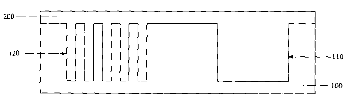
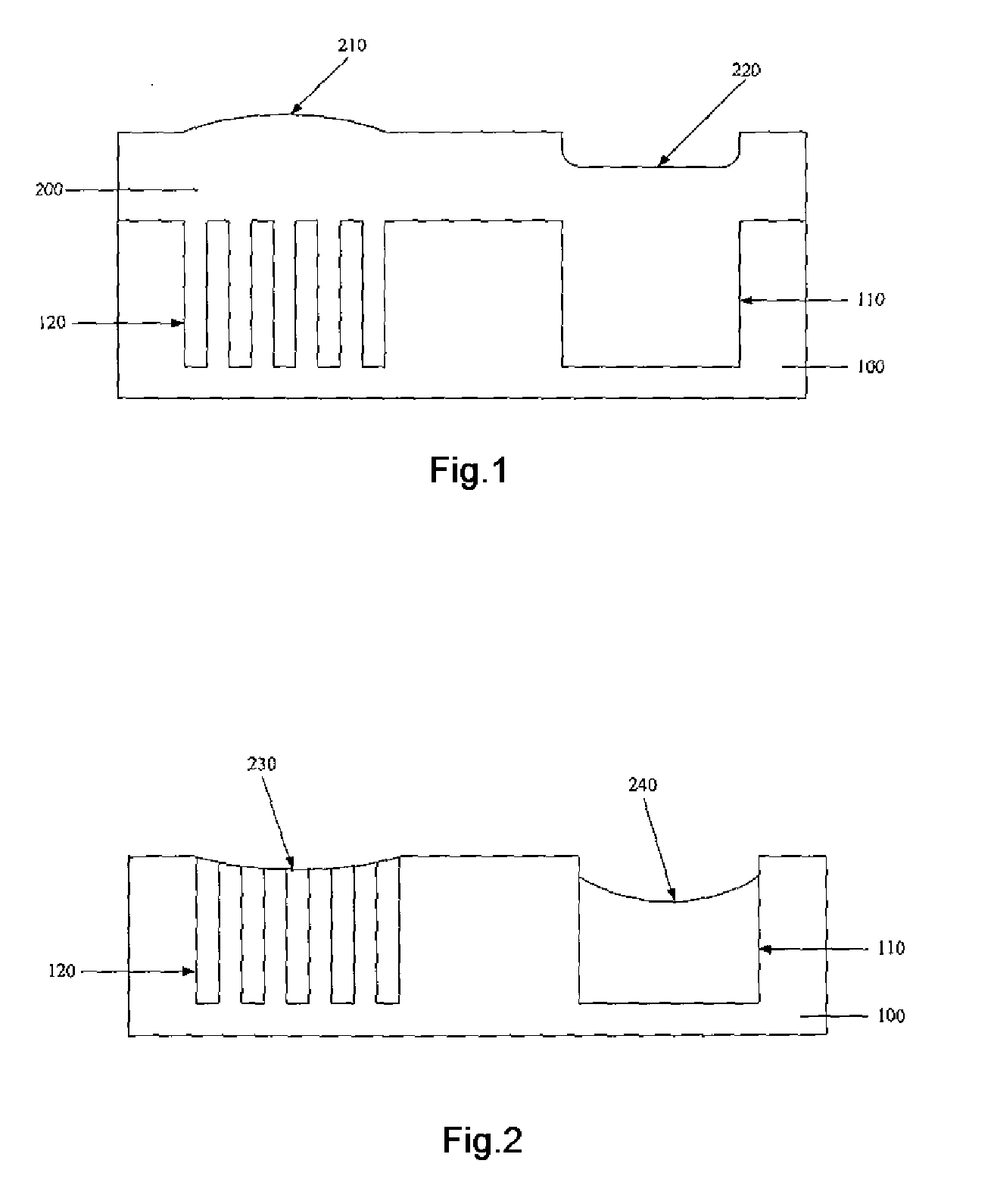
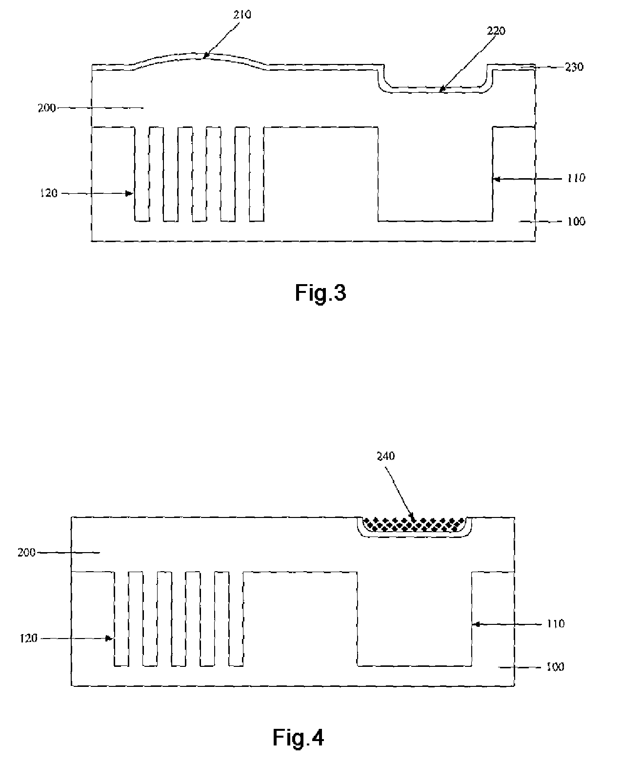
[0033]FIG. 3 to FIG. 6 are schematic cross-section views of the device for illustrating the preferred embodiments of the present invention. The schematic views are only examples, which do not intend to limit the scope of the present invention. At first, as shown in FIG. 3, the dielectric layer 100 is an inorganic s...


PUM

PropertyMeasurementUnit
temperatureaaaaaaaaaa
dielectricaaaaaaaaaa

Abstract

Disclosed is a chemical mechanical polishing planarization method for copper surface, including the following steps: depositing a dielectric layer on the copper surface, and polishing the copper surface having the dielectric layer thereon. The method for planarizing a copper surface by chemical mechanical polishing process according to the present invention can achieve the planarization of the surfaces of both the copper and the dielectric layer, so as to avoid the occurrence of the dishing phenomenon.

Description

FIELD OF THE INVENTION[0001]The present invention generally relates to the technical field of semiconductor manufacture, and more particularly, to a chemical mechanical polishing (CMP) process for planarizing copper damascene surface.DESCRIPTION OF THE RELATED ART[0002]With the rapid development of semiconductor manufacturing technology, the critical dimension (CD) of semiconductor device has reached a deep-submicron level. It is required to reduce the time-delay caused by impedance, in order to increase the operating rate of a chip. Accordingly, most of the dielectrics used in a semiconductor device have a low dielectric constant and copper metal is widely used as an interconnection material, in order to reduce the resistance of the metal wire. The interconnection structure is typically formed by a damascene process, that is, by etching one or more dielectric layers on the substrate to form the via or trench and then depositing metal into the via or trench. Although the resistance ...

Claims


Application Information

Patent Timeline
Patent Type & Authority Applications(United States)
IPC IPC(8): B44C1/22
CPCH01L21/31116H01L21/3212
Inventor ZHU, XUANTSAI, MENGFENG
Owner SEMICON MFG INT (SHANGHAI) CORP
Why Eureka
Try Eureka