

Optical Device, Method for Producing Master for Use in Producing Optical Device, and Photoelectric Conversion Apparatus
a technology of optical devices and masters, applied in the manufacture of discharge tubes/lamps, final product manufacturing, optical radiation measurement, etc., to achieve the effects of improving power generation efficiency in photoelectric conversion potion, excellent light transmittance properties, and improving light utilization efficiency
- Summary
- Abstract
- Description
- Claims
- Application Information
AI Technical Summary
Benefits of technology
Problems solved by technology
Method used
Image

Examples
first embodiment
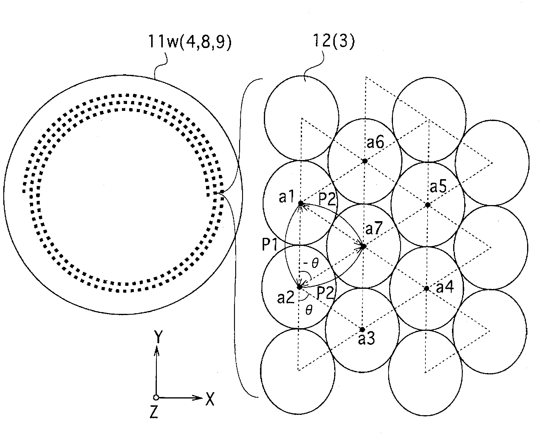
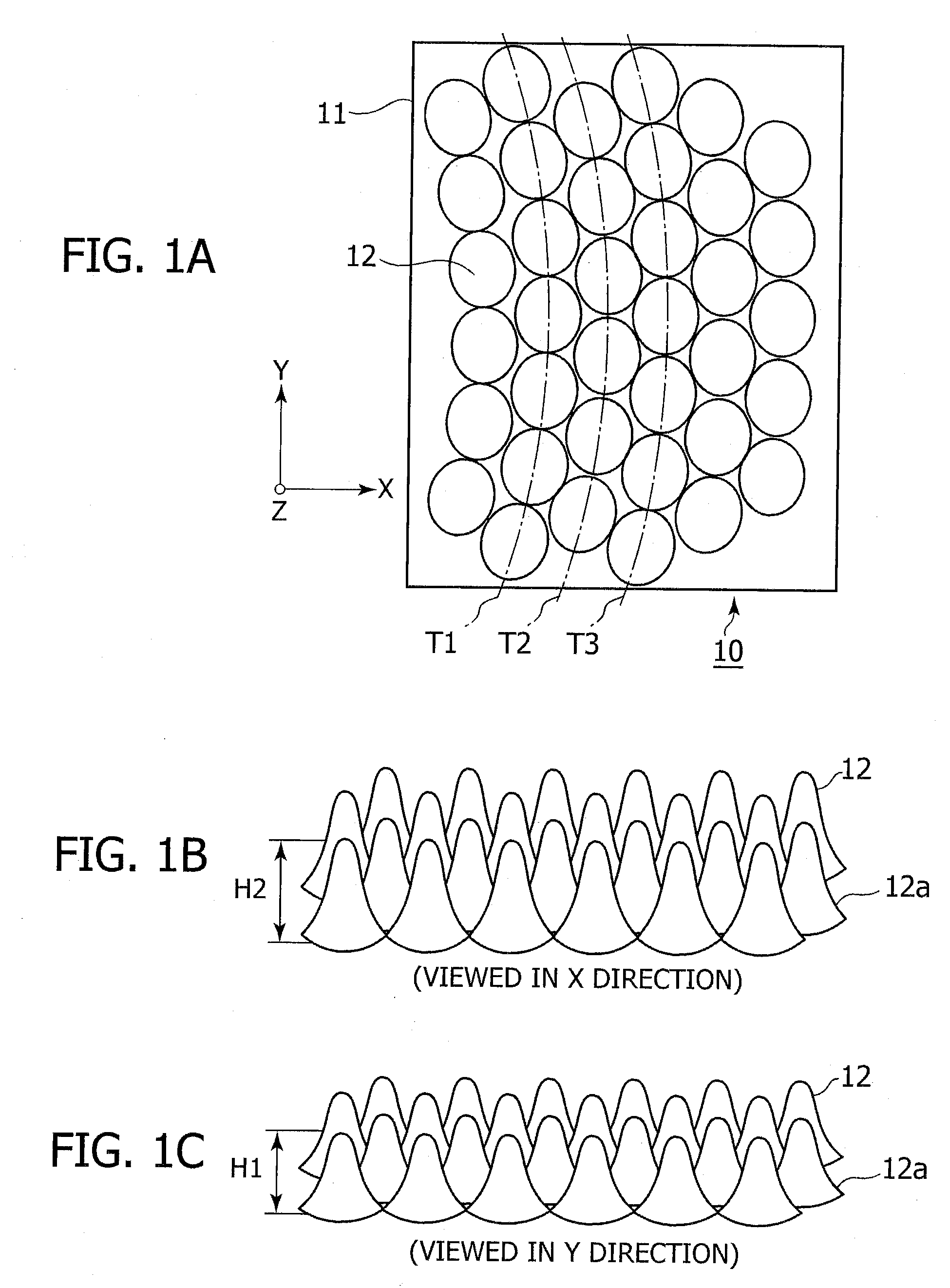
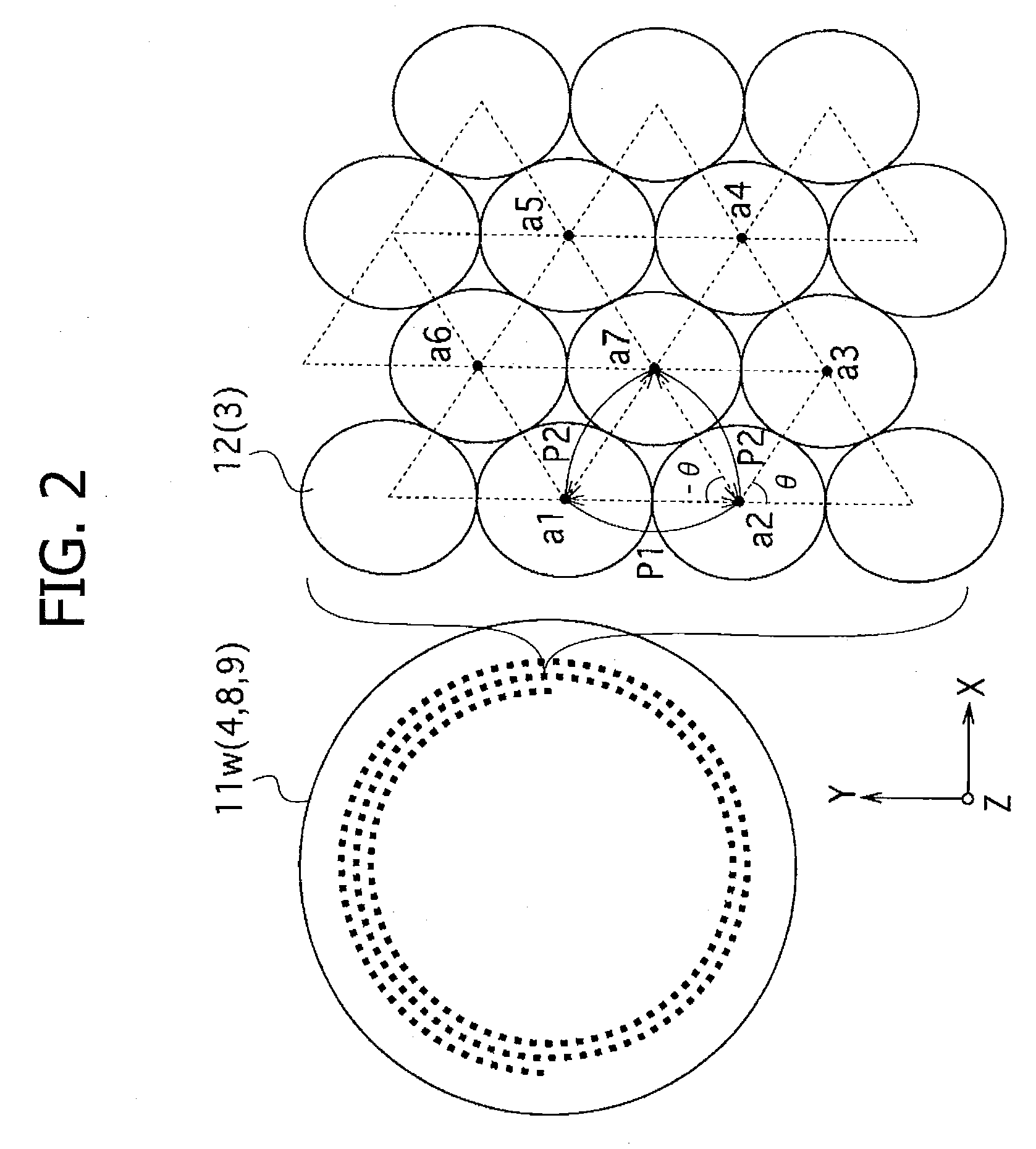
[0073]FIG. 1 is diagrammatic views showing the construction of an optical device 10 according to a first embodiment of the present invention. Here, FIG. 1A is a main portion top view of the optical device 10, FIG. 1B is a main portion perspective view of the optical device 10 viewed from the X direction in FIG. 1A, and FIG. 1C is a main portion perspective view of the optical device 10 viewed from the Y direction in FIG. 1A.
[0074]The optical device 10 according to the present embodiment has, a configuration (subwavelength configuration) in which a number of structures 12 having higher portions are arranged at a fine pitch equal to or shorter than the wavelength of visible light on the surface of a base 11. Here, the terms “a wavelength equal to or shorter than the wavelength of visible light” used here is a wavelength equal to or shorter than around 400 nm. The optical device 10 has a function of preventing the reflection at an interface between the structures 12 and the surrounding...
second embodiment
[0123]Subsequently, a second embodiment of the present invention is described.
[0124]FIG. 7 is diagrammatic process cross-sectional views of a main portion for explaining a method for producing an optical device having the sub-wavelength structures formed on the both surfaces of the base 11. FIG. 7A is a step for forming a pattern of the resist layer 2 on the surface of quartz substrate 1, FIG. 7B is a step for producing the master 4 for use in producing an optical device by performing etching through use of the patterned resist layer 2 as a mask, the master having an uneven structure including the lower portions 3 on the surface of the substrate 1, FIG. 7C is a step for producing a replica substrate 8 for use in forming an optical device in which the uneven structure including the light cure resin 7 is transferred on the transparent substrate 6, FIG. 7D is a step for producing the mold 9 for use in forming an optical device, which is obtained in that a conducting film is grown to pl...
third embodiment
[0128]FIG. 8 shows a third embodiment of the present invention. In the present embodiment, a dye-sensitized solar cell 50 in which the optical device 40 having the construction explained in the second embodiment is used as a light guide window is described as an example.
[0129]The dye-sensitized solar cell 50 of the present embodiment includes a light guide window 40 having a transparent conductive film 41 and a laminated body in which a metal-oxide semiconductor layer 45 and an electrolyte layer 46 are provided between the (transparent) conductive film 42 which is opposite to the transparent conductive film 41 and a substrate 44 having a current collection material 43. The semiconductor layer 45 includes, for example, oxide semiconductor materials and sensitizing dyes. Further, the transparent conductive film 41 and the conductive film 42 are connected via a conductor wire to form a current circuit having an ammeter 47.
[0130]The light guide window 40 is formed by using a glass subst...
PUM
| Property | Measurement | Unit |
|---|---|---|
| Nanoscale particle size | aaaaa | aaaaa |
| Nanoscale particle size | aaaaa | aaaaa |
| Nanoscale particle size | aaaaa | aaaaa |
Abstract
Description
Claims
Application Information