Method for manufacturing compound material wafer and corresponding compound material wafer

a technology of compound material and manufacturing method, which is applied in the direction of basic electric elements, electrical apparatus, semiconductor devices, etc., can solve the problems of reducing the need for extensive additional steps, and the state of the art, so as to speed up the process, improve the crystalline quality of the donor substrate, and increase the number of reuses of the donor substrate.

Inactive Publication Date: 2008-10-30
S O I TEC SILICON ON INSULATOR THECHNOLOGIES
View PDF14 Cites 3 Cited by
  • Summary
  • Abstract
  • Description
  • Claims
  • Application Information

AI Technical Summary

Benefits of technology

[0011]Depending on the thickness of the thermally grown layer it is even possible to carry out the layer forming process step at temperatures of up to 1000° C., to speed up the process. According to a variant it is preferable to keep the growth temperature at values of less than 950° C., preferably at values of less than 850° C., in which case the time to grow a layer of the same thickness is longer, however, the crystalline quality of the donor substrate remains better.
[0012]According to a preferred embodiment, the attaching can occur at the surface of the first or third insulating layer of the donor substrate. Thus, once the first or third insulating layer is provided, the donor substrate does not see a further layer forming process which could affect its crystalline quality. Thus, the number of reuses of the donor substrate can be further enhanced. If further layers are necessary in the compound material wafer, these additional layers are preferably provided over the handle substrate.
[0013]Another embodiment of the invention relates to a method for manufacturing compound material wafers which comprises the steps of providing a donor substrate, forming a first insulating layer upon the donor, forming a predetermined splitting area in the donor substrate to define a layer to be transferred and a remainder of the donor substrate, attaching the donor substrate to a handle substrate, and detaching the donor substrate at the predetermined splitting area, thereby transferring the defined layer of the donor substrate onto the handle substrate to form a compound material wafer. The method is preferably repeated at least three to ten times, with the remainder of the donor substrate after a detaching step being provided as the initial donor substrate for the next repeat of the steps. As mentioned above, it appeared that the decisive step concerning the number of possible reuses of the donor substrate is the step of forming the insulating layer over the initial donor substrate. Surprisingly a deposition process to form the insulating layer lead to a higher number of possible reuses for the same insulator thickness than compared to cases where the insulating layer was formed using the standard thermal process because the deposition process minimizes introducing heat into the donor substrate that would reduce the crystalline quality of the donor substrate remainder.
[0014]According to a preferred embodiment, the inventive method can furthermore comprise an additional step of densifying the insulating layer after detaching, in particular using a thermal treatment under a neutral atmosphere. Typically, deposited layers are less dense than thermally grown layers, e.g. they are porous, but this inconvenience can be overcome by carrying out a thermal treatment under neutral atmosphere, in particular during a few hours. As the densification takes place after detachment from the donor substrate has occurred, the crystalline quality of the donor substrate can not be negatively affected by this thermal treatment.
[0015]Advantageously the depositing step can be carried out at low temperature, in particular at less than 750° C., in particular in the range of 400° C. to 600° C. In this temperature range throughput can be kept high.
[0016]According to a preferred embodiment, the attaching can occur at the surface of the first insulating layer of the donor substrate. In this way it is ensured that the donor substrate does not see any further thermal treatment which may influence its crystalline quality, so that the number of reuses of the donor substrate can be further enhanced. If further layers are necessary in the compound material wafer, these additional layers are preferably provided over the handle substrate.

Problems solved by technology

In addition, the necessity of extensive additional steps, like those proposed by the state of the art, become obsolete.
It was found out that one of the decisive steps concerning the number of possible reuses, is the thermal treatment step to obtain the insulating layer as this step leads to a decrease in the crystalline quality of the donor substrate.

Method used


Image

  • Method for manufacturing compound material wafer and corresponding compound material wafer
  • Method for manufacturing compound material wafer and corresponding compound material wafer
  • Method for manufacturing compound material wafer and corresponding compound material wafer

Examples


first embodiment

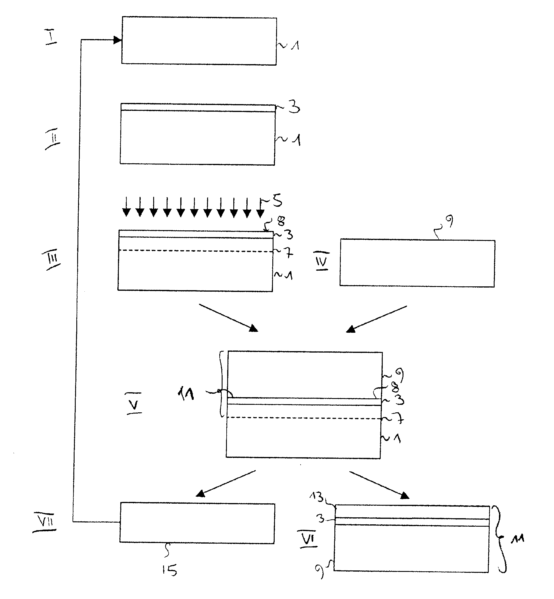
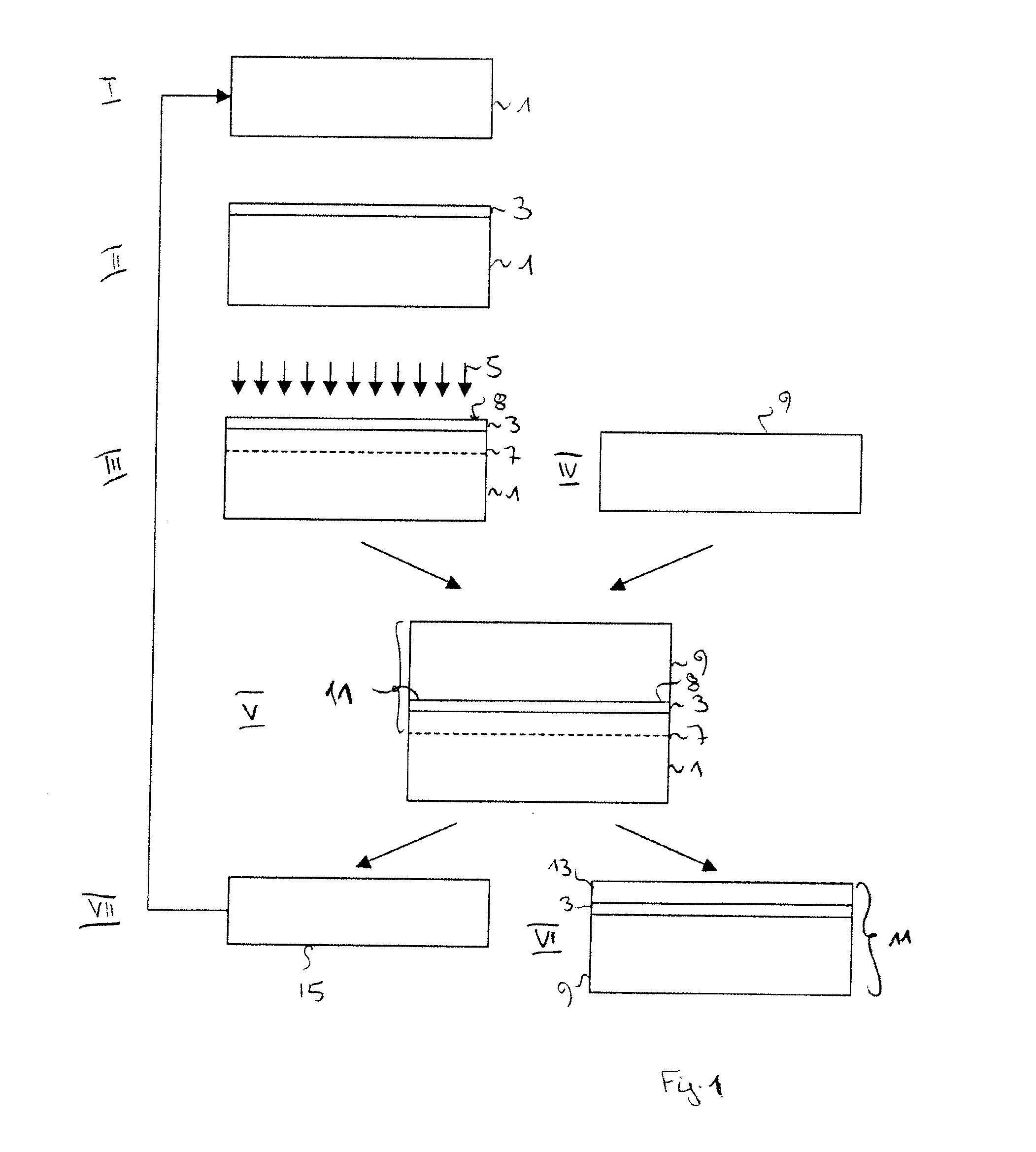
[0031]FIG. 1 illustrates the inventive method for manufacturing compound material wafers. The method will be described for a silicon on insulator (SOI) type compound material wafer. This, nevertheless, only serves as an example and the inventive method is also applicable to other types of material compound wafers.

[0032]Step I of the inventive method consists in providing an initial donor substrate 1 which, in the preferred embodiment, is a silicon wafer. Step II illustrates a step of forming an insulating layer 3 on the silicon wafer 1. Here the insulating layer 3 is a silicon dioxide layer (SiO2), which is formed by a thermal treatment under oxidizing conditions. According to this first embodiment of the invention the insulating layer 3 is thermally grown to a thickness of at most 500 Å.

[0033]In Step III, atomic species 5, in particular, hydrogen or rare gas ions such as helium, are implanted under predetermined dose and energy conditions through the insulating layer 3 to create a ...

second embodiment

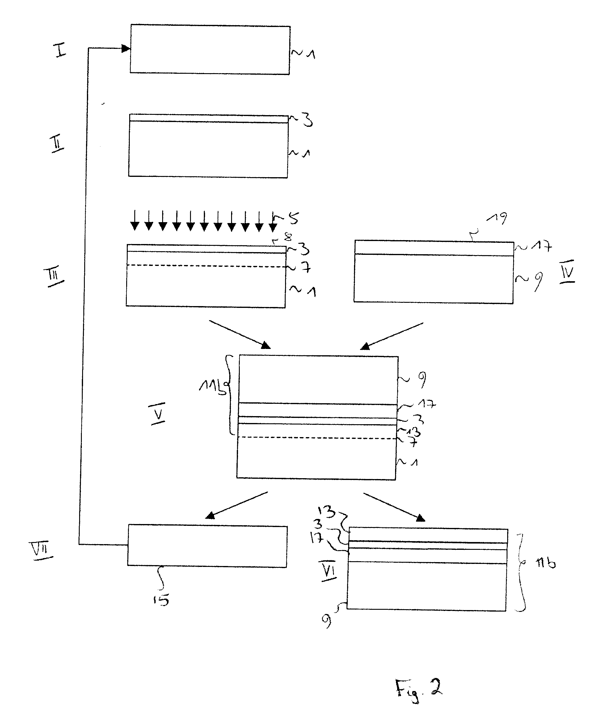
[0056]The third insulating layer 21 is a deposited layer, wherein deposition is preferably carried out at relatively low temperatures, in particular, at less than 750° C., more in particular, in a range of 400° C. to 600° C. By doing so the thermal budget seen by the donor substrate 1 is kept low, so that the donor substrate can still be reused more than 3 times, in particular five to ten times. Like in the second embodiment, it again becomes possible to obtain an insulating layer with a thickness, which can be freely chosen as a function of the applications for which the compound material wafer is intended for, as the insulating layer thickness corresponds to the sum of the thickness of the first insulating layer 3 and the thickness of the third insulating layer 17, the later having a thickness that can be chosen freely.

[0057]Apart from that, all the other advantages and variants as disclosed with respect to the first and second embodiments are also achieved in this embodiment.

[005...

sixth embodiment

[0071]FIG. 6 illustrates the inventive method for fabricating a hybrid orientation wafer. In contrast to the previous embodiments, this embodiment does not use any insulating layers. As a consequence, the donor substrate is not subject to a thermal layer forming treatment, which could negatively influence the crystalline quality of the donor substrate. Therefore also in this embodiment it is possible to reuse the donor substrate more than three times.

[0072]Step I of the method according to this embodiment relates to providing an initial donor substrate 51 which has a first crystal orientation. This can for example be a silicon wafer of (1,0,0) or (1,1,0) crystalline orientation.

[0073]Step II then illustrates the implantation of atomic species 5 into the donor substrate 51 to create a predetermined splitting area 7 in this substrate 51. The conditions under which implantation occurs are comparable to the ones of the previously described embodiments and are not repeated here as they a...


PUM

PropertyMeasurementUnit
temperatureaaaaaaaaaa
temperaturesaaaaaaaaaa

Abstract

The invention relates to methods for manufacturing compound material wafers, in particular silicon on insulator wafers, by the steps of providing a donor substrate, forming an insulating layer, providing a handle substrate, creating a predetermined splitting area in the donor substrate, attaching the donor substrate to the handle substrate and detaching at the predetermined splitting area to achieve the compound material wafer. In order to be able to more often reuse the remainder of the donor substrate in subsequent manufacturing runs, various embodiments are disclosed, such as the insulating layer can be provided on the donor substrate at a maximum thickness of 500 A, or that the insulating layer can be provided by deposition or only upon the handle substrate. Alternatively, no insulating layer is provided so that the donor and handle substrates can have different crystal orientations.

Description

BACKGROUND ART[0001]The invention relates to a method for manufacturing compound material wafers, in particular silicon on insulator type wafers and corresponding compound material wafers.[0002]Compound material wafers, in particular silicon on insulator (SOI) wafers, are semiconductor substrates which, in modern semiconductor devices, play a decisive role to ensure ever higher speed as smaller dimensions are enabled. The process to fabricate such compound material wafers has, however, to satisfy at least two basic requirements. First, a good crystalline quality needs to be satisfied over essentially the entire surface of the wafer in the layered structure and, second, the fabrication needs to be carried out without incurring excessive costs.[0003]One way to satisfy the above mentioned requirements is the so called SMART-CUT® fabrication process in which a layer from a donor substrate is transferred onto a handle substrate. This is achieved by bonding the two substrates and detachin...

Claims


Application Information

Patent Timeline
Patent Type & Authority Applications(United States)
IPC IPC(8): H01L21/20
CPCH01L21/02032H01L21/76254H01L21/20H01L21/762H01L27/12
Inventor REYNAUD, PATRICKKONONCHUK, OLEG
Owner S O I TEC SILICON ON INSULATOR THECHNOLOGIES
Why Eureka
Try Eureka