Solar cell absorber layer formed from metal ion precursors

a metal ion precursor and solar cell technology, applied in the field of photovoltaic devices, can solve the problems of poor surface coverage, low throughput and high cost of vacuum deposition equipment, and the difficulty of achieving the precise stoichiometric composition over relatively large substrate areas in a manufacturing setting using traditional vacuum deposition processes

Inactive Publication Date: 2008-11-13
AERIS CAPITAL SUSTAINABLE IP
View PDF6 Cites 160 Cited by
  • Summary
  • Abstract
  • Description
  • Claims
  • Application Information

AI Technical Summary

Benefits of technology

[0014]In another embodiment of the present invention, a method is provided comprising depositing a solution on a substrate to form a precursor layer. The solution comprises of at least one polar solvent and at least one Group IB and/or IIIA hydroxide. The method may include processing the precursor layer in one or more steps to form a photovoltaic absorber layer, wherein the solution is without an organic binder. Creating the absorber layer may include processing the precursor layer into a solid film and then thermally reacting the solid film in an atmosphere containing at least an element of Group VIA of the Periodic Table to form the photovoltaic absorber layer. Creating the absorber layer may include thermal reaction of the precursor layer in an atmosphere containing at least an element of Group VIA of the Periodic Table to form the photovoltaic absorber layer.
[0015]In another embodiment of the present invention, a method is provided comprising depositing a solution on a substrate to form a precursor layer. The solution comprises of at least one apolar solvent and at least one salt of an element entering the composition of the absorber layer, wherein the solution is without an organic binder and wherein the salt remains as un-dissolved particles in the apolar solvent. The precursor layer may be processed in one or more steps to form a photovoltaic absorber layer. Creating the absorber layer may include processing the precursor layer into a solid film and then thermally reacting the solid film in an atmosphere containing at least an element of Group VIA of the Periodic Table to form the photovoltaic absorber layer. Creating the absorber layer may include thermal reaction of the precursor layer in an atmosphere containing at least an element of Group VIA of the Periodic Table to form the photovoltaic absorber layer.
[0016]In another embodiment of the present invention, a method of forming an absorber layer is provided comprising of depositing a solution on a substrate to form a precursor layer. The solution comprises of at least one polar solvent and at least one salt of an element entering the composition of the absorber layer, wherein the solution is without an organic b

Problems solved by technology

These electronic devices have been traditionally fabricated using silicon (Si) as a light-absorbing, semiconducting material in a relatively expensive production process.
A central challenge in cost-effectively constructing a large-area CIGS-based solar cell or module involves reducing processing costs and material costs.
The nature of vacuum deposition processes requires equipment that is generally low throughput and expensive.
Vacuum deposition processes are also typically carried out at high temperatures and for extended times. Furthermore, achieving precise stoichiometric composition over relatively large substrate areas desired in a manufacturing setting is difficult using traditional vacuum-based deposition processes.
Traditional sputtering or co-evaporation techniques are limited to line-of-sight and limited-area sources, tending to result in poor surface coverage and non-uniform three-dimensional distribution of the elements.
These non-uniformities can occur over the nano-, meso-, and/or macroscopic scales and alters the local stoichiometric ratios of the absorber layer, decreasing the potential power conversion efficiency of the complete cell or module.
Additionally, vacuum deposition processes typically have a low material yield, often depositing material on non-targeted surfaces.
A huge disadvantage of techniques that directly nucleate and grow a thin film from solution is the importance of the nature and cleanliness of the substrate surface to allow uniform nucleation and growth of high-quality multinary compound films.
Incorporation of unwanted impurities from solution into the thin fi

Method used


Image

  • Solar cell absorber layer formed from metal ion precursors
  • Solar cell absorber layer formed from metal ion precursors
  • Solar cell absorber layer formed from metal ion precursors

Examples


embodiment 1

[0060]This embodiment shows the use of Group IB and / or IIIA hydroxide(s) in a polar solvent with a binder.

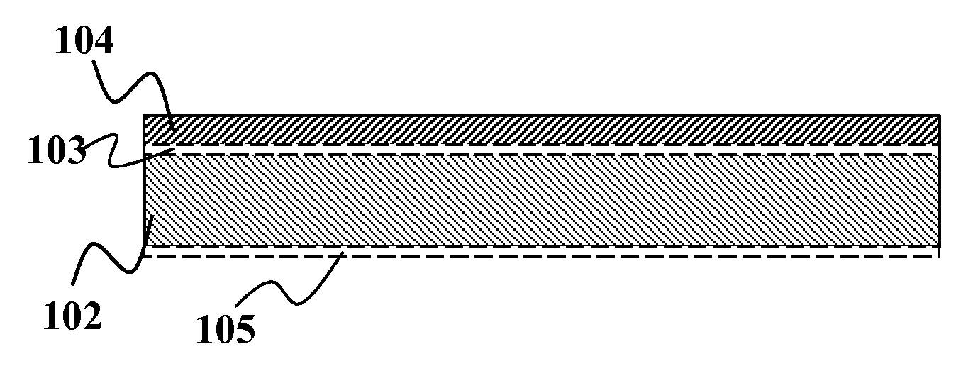
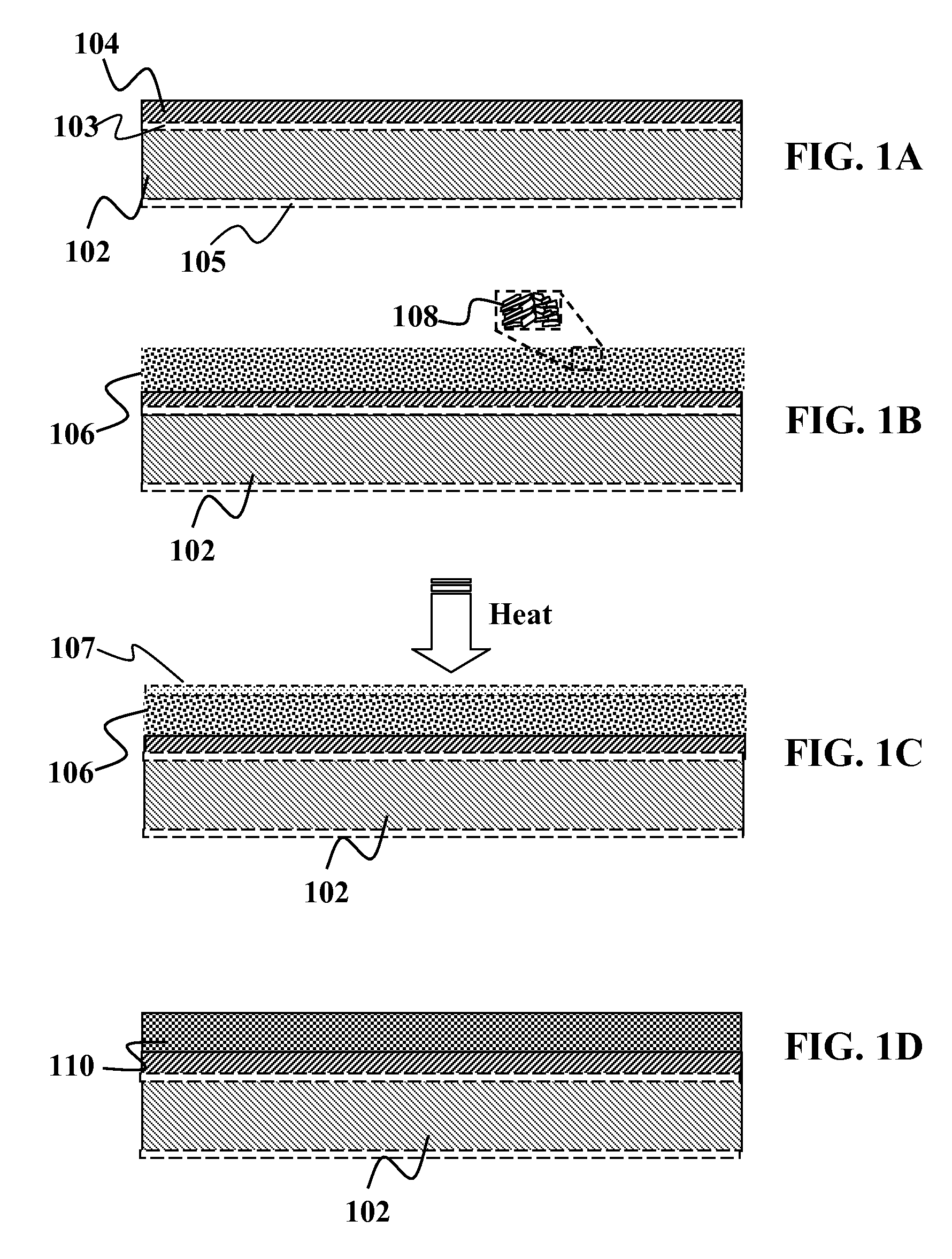
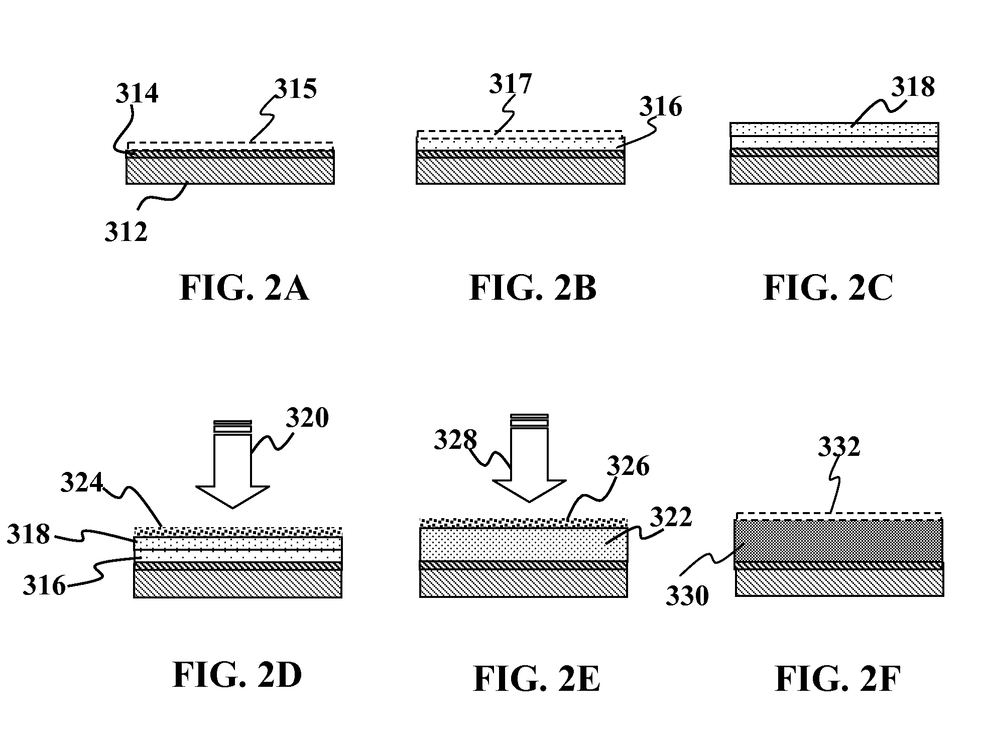
[0061]A substrate such as an aluminum foil layer with an Mo coating on one side or both sides is provided. Optionally, other metal foils such as stainless steel or copper may also be used in place of the aluminum foil. The foil itself (prior to adding the Mo coating) may include a diffusion barrier layer above and / or below the foil. An approximately 0.5-2.5 um thick layer of a precursor material may be solution deposited over the Mo layer. The precursor material may comprise of a dispersion of nanoparticles of, copper-gallium, elemental gallium, and indium hydroxide. One such example would be a combination of Cu85Ga15, In(OH)3, and elemental gallium. Optionally, the dispersion may comprise of copper nanoparticles and indium-gallium hydroxide. Still optionally, the dispersion may comprise of copper-gallium and indium hydroxide without separate elemental gallium. In one embodiment...

embodiment 2

[0065]This embodiment shows the use of a Group IB and / or IIIA hydroxides in a polar solvent without a binder. Without the binder, the dispersion and / or process is changed so that the process conditions do not require removal of the binder or residues from the binder from the electrodes and / or absorber, and / or junction partner.

[0066]A substrate such as an aluminum foil layer with an Mo coating on one side or both sides is provided. Optionally, other metal foils such as stainless steel or copper may also be used in place of the aluminum foil. The foil itself (prior to adding the Mo coating) may include a diffusion barrier layer above and / or below the foil. An approximately 0.5-2.5 um nm thick layer of a precursor material may be solution deposited over the Mo layer. The precursor material may comprise of a dispersion of copper nanoparticles, gallium, and indium hydroxide. One such example would be a combination of a Cu—Ga alloy, like Cu75Ga25, indium hydroxide, with or without additio...

embodiment 3

[0069]This embodiment shows the use of a Group IB and / or IIIA hydroxides in an apolar solvent with a binder. Some suitable apolar solvents include but are not limited to: halogenated solvents like carbon tetrachloride, ethers like diethylether, aromatics like toluene, and the like.

[0070]A substrate such as an aluminum foil layer with an Mo coating on one side or both sides is provided. Optionally, other metal foils such as stainless steel or copper may also be used in place of the aluminum foil. The foil itself (prior to adding the Mo coating) may include a diffusion barrier layer above and / or below the foil. An approximately 0.5-3.5 um nm thick layer of a precursor material may be solution deposited over the Mo layer. The precursor material may comprise of a dispersion of copper nanoparticles, gallium, and indium hydroxide. One such example would be a combination of a Cu—In alloy, like Cu70In30, indium hydroxide, with elemental gallium. Optionally, the dispersion may include copper...


PUM


Abstract

Methods and devices are provided for forming an absorber layer. In one embodiment, a method is provided comprising of depositing a solution on a substrate to form a precursor layer. The solution comprises of at least one polar solvent, at least one binder, and at least one Group IB and/or IIIA hydroxide. The precursor layer is processed in one or more steps to form a photovoltaic absorber layer. In one embodiment, the absorber layer may be created by processing the precursor layer into a solid film and then thermally reacting the solid film in an atmosphere containing at least an element of Group VIA of the Periodic Table to form the photovoltaic absorber layer. Optionally, the absorber layer may be processed by thermal reaction of the precursor layer in an atmosphere containing at least an element of Group VIA of the Periodic Table to form the photovoltaic absorber layer.

Description

CROSS-REFERENCE TO RELATED APPLICATION[0001]This application claims the benefit of priority to U.S. Provisional Application Ser. No. 60 / 887,582 filed Jan. 31, 2007 and fully incorporated herein by reference for all purposes.FIELD OF THE INVENTION[0002]This invention relates generally to photovoltaic devices, and more specifically, to use of metal ion precursors in forming photovoltaic devices.BACKGROUND OF THE INVENTION[0003]Solar cells and solar modules convert sunlight into electricity. These electronic devices have been traditionally fabricated using silicon (Si) as a light-absorbing, semiconducting material in a relatively expensive production process. To make solar cells more economically viable, solar cell device architectures have been developed that can inexpensively make use of thin-film, preferably non-silicon, light-absorbing semiconductor materials such as copper-indium-gallium-selenide (CIGS).[0004]A central challenge in cost-effectively constructing a large-area CIGS-b...

Claims


Application Information

Patent Timeline
IPC IPC(8): B05D5/12
CPCH01L31/03928H01L31/06H01L31/0749Y02E10/541Y02P70/50
Inventor VAN DUREN, JEOREN K. J.SAGER, BRIAN M.ROBINSON, MATTHEW R.
Owner AERIS CAPITAL SUSTAINABLE IP
Why Eureka
Try Eureka