Irradiating apparatus, semiconductor device manufacturing apparatus, semiconductor device manufacturing method, and display device manufacturing method

Inactive Publication Date: 2008-11-13
SONY CORP
View PDF10 Cites 9 Cited by
  • Summary
  • Abstract
  • Description
  • Claims
  • Application Information

AI Technical Summary

Benefits of technology

[0011]It is accordingly desirable to provide an irradiating apparatus that can irradiate an irradiation object with laser light without being affected by individual difference of a semiconductor laser or the like, by optimizing a focal position for a necessary beam diameter, a semiconductor device manufacturing apparatus, a semiconductor device manufacturing method, and a display device manufacturing method.
[0013]With the irradiating apparatus having the above-described constitution, the focal position of the irradiating optical system is not on the irradiation object but is defocused from the surface of the irradiation object by the distance z, and the amount of defocus is optimized for the necessary irradiation beam radius w. Thus, an irradiating optical system that can provide the desired irradiation beam radius w without being affected by individual difference in angle of divergence of the semiconductor laser and which achieves a greatest depth of focus is realized.
[0014]According to the present invention, a desired beam diameter can be obtained without being affected by individual difference in angle of divergence of the semiconductor laser. It is therefore possible to avoid causing a difference in conditions for irradiation with laser beam light after the replacement of the semiconductor laser, eliminate a need for the setting of conditions such as focus adjustment and the like, and expect for example an improvement in processing efficiency attendant on the simplification of a device constitution and the simplification of a processing procedure as a result of obviating a need for a Z-stage and the like. In addition, also when an apparatus including a semiconductor laser and an irradiating optical system is mass-produced, for example, there is no effect of individual difference in angle of divergence of the semiconductor laser. Therefore the yield of the product is improved greatly, which also leads to a reduction in cost of the product.

Problems solved by technology

However, the following problems may occur when irradiation is performed with laser light using the irradiating optical system based on the existing technique described above.
The irradiating optical system cannot correct the effect.

Method used


Image

  • Irradiating apparatus, semiconductor device manufacturing apparatus, semiconductor device manufacturing method, and display device manufacturing method
  • Irradiating apparatus, semiconductor device manufacturing apparatus, semiconductor device manufacturing method, and display device manufacturing method
  • Irradiating apparatus, semiconductor device manufacturing apparatus, semiconductor device manufacturing method, and display device manufacturing method

Examples


Embodiment Construction

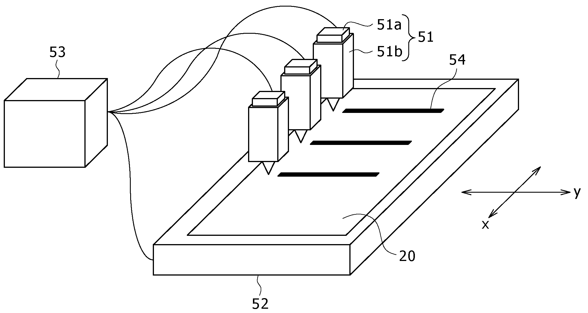
[0029]An irradiating apparatus, a semiconductor device manufacturing apparatus, a semiconductor device manufacturing method, and a display device manufacturing method according to embodiments of the present invention will hereinafter be described with reference to the drawings.

[0030]An outline of a semiconductor device manufactured using irradiation with laser light will first be described.

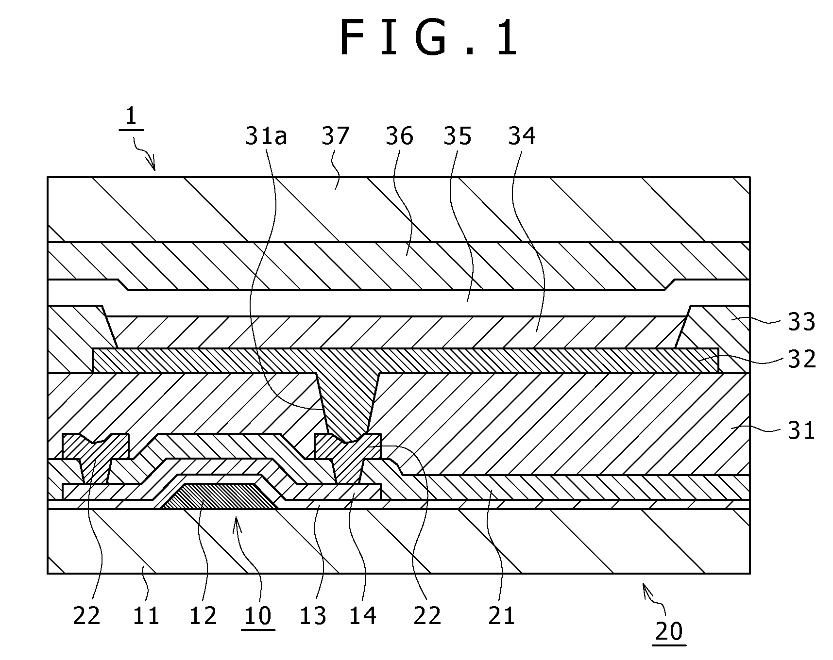
[0031]The semiconductor device to be described in the following is obtained through modification of an amorphous silicon film (amorphous silicon will hereinafter be described as “a-Si”) from an amorphous state to a polycrystalline state, that is, modification of the amorphous silicon film from a-Si into a polycrystalline silicon film (polysilicon will hereinafter be described as “p-Si”). Specifically, a TFT, which is a thin film semiconductor device, is cited as an example of the semiconductor device.

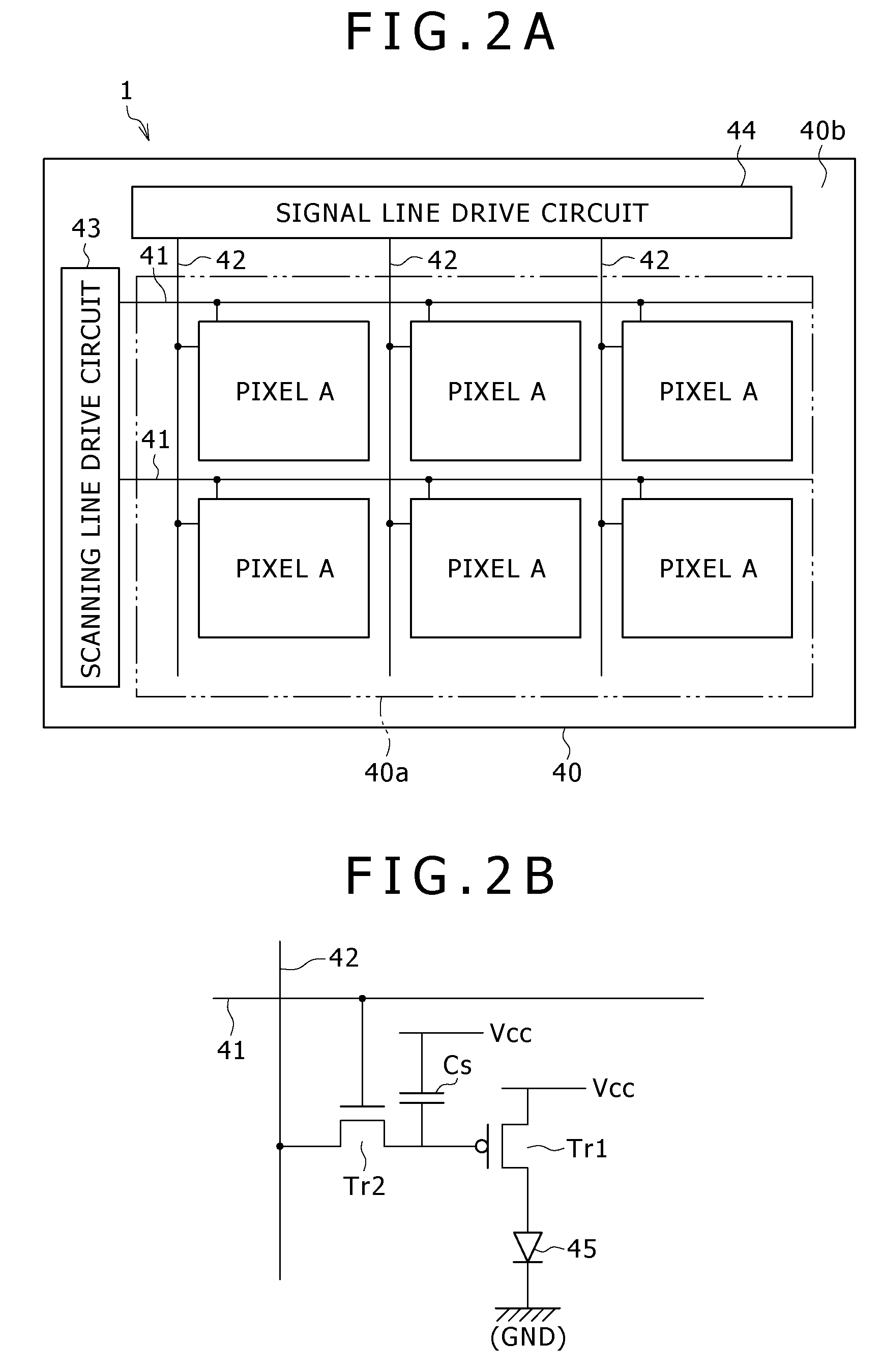
[0032]The TFT is for example used to form a display device such as an active matrix type liquid cr...


PUM

PropertyMeasurementUnit
Lengthaaaaaaaaaa
Diameteraaaaaaaaaa

Abstract

An irradiating apparatus for irradiating an irradiation object with beam light emitted from a semiconductor laser, wherein letting w be a radius of a beam for irradiating the irradiation object, Δ be a rate of individual difference in angle of divergence of the semiconductor laser, and λ be beam wavelength of the semiconductor laser, a focal position of an irradiating optical system interposed between the semiconductor laser and the irradiation object is defocused such that a distance z between the focal position and the irradiation object isz=π·w2λ·1-Δ2(1-Δ2)2+1[Equation1]

Description

CROSS REFERENCES TO RELATED APPLICATIONS[0001]The present invention contains subject matter related to Japanese Patent Application JP 2007-127098, filed in the Japan Patent Office on May 11, 2007, the entire contents of which being incorporated herein by reference.BACKGROUND OF THE INVENTION[0002]1. Field of the Invention[0003]The present invention relates to an irradiating apparatus for performing irradiation with beam light using a semiconductor laser as a light source, a semiconductor device manufacturing apparatus for manufacturing a semiconductor device using irradiation with the beam light, a semiconductor device manufacturing method, and a display device manufacturing method.[0004]2. Description of the Related Art[0005]It is known that when an active matrix type liquid crystal display device, an organic electroluminescent display device (hereinafter referred to as an “organic EL display”) using an organic electroluminescent element (hereinafter referred to as an “organic EL e...

Claims


Application Information

Patent Timeline
IPC IPC(8): H01L21/428H01S5/00G02B27/00H01L21/268
CPCB23K26/0648B23K26/0665B23K26/067B23K26/0676B23K26/0853B23K2201/40G02F1/1303G02F2202/104H01L21/02675H01S5/005H01S5/4012H01S5/4025B23K2101/40H01L21/324
Inventor TSUKIHARA, KOICHI
Owner SONY CORP
Why Eureka
Try Eureka