

Micro-sample processing method, observation method and apparatus
a processing method and micro-sample technology, applied in material analysis using wave/particle radiation, instruments, nuclear engineering, etc., can solve the problems of reducing the throughput of the process, reducing the imaging resolution, and deformation at the observed portion, so as to reduce sample damage, suppress damage and deformation, and check the structure of the cross-section
- Summary
- Abstract
- Description
- Claims
- Application Information
AI Technical Summary
Benefits of technology
Problems solved by technology
Method used
Image

Examples
first embodiment
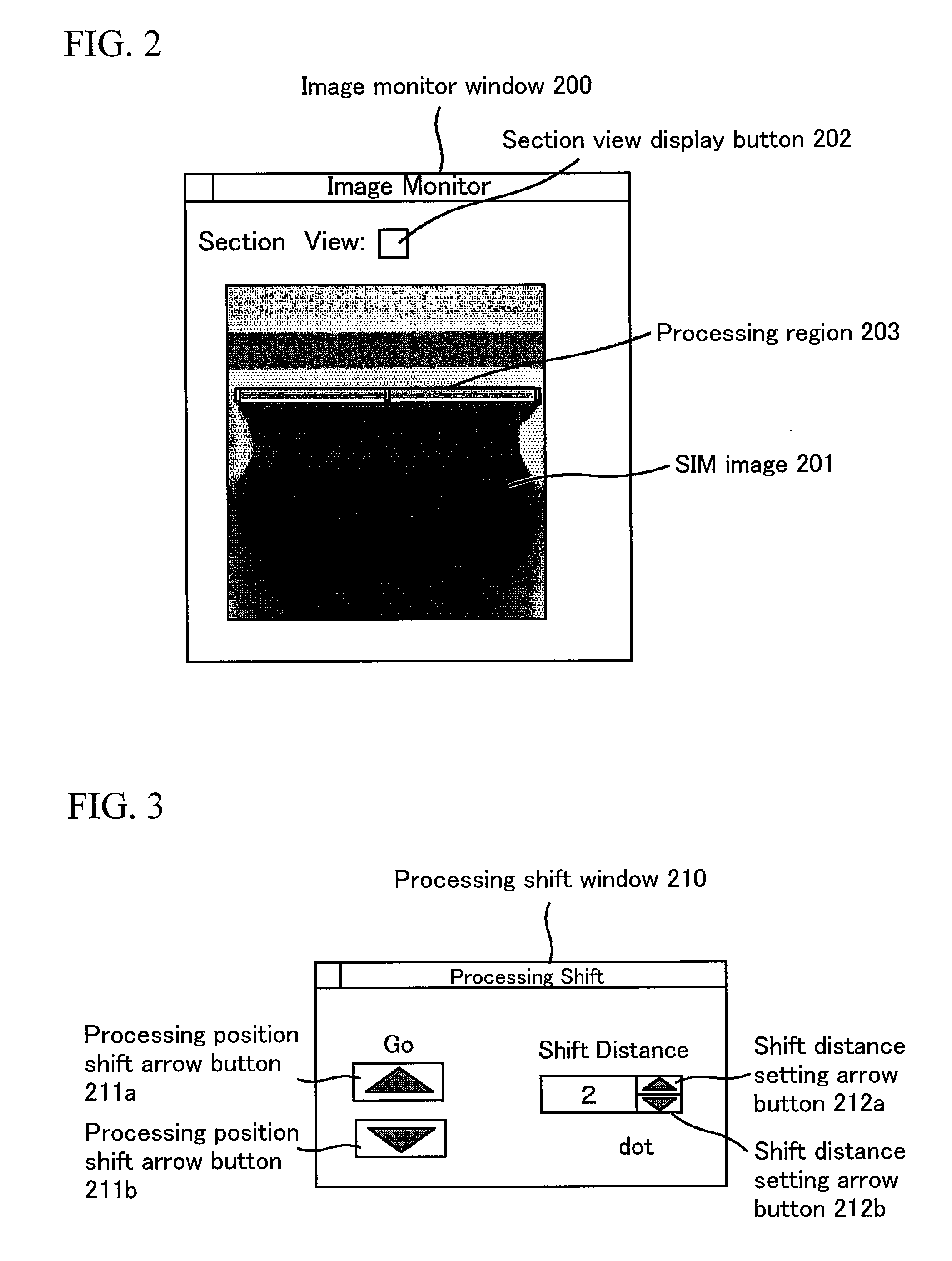
[0032]FIG. 5 shows a construction of an FIB apparatus used in a first embodiment of the present invention. An FIB 3 generated by the FIB column 100 is focused on and scanned across a sample 1. Secondary electrons 2 emitted from the sample are detected by a detector 101, converted to digital values via a signal processing unit 112, and stored in an image memory in an image displaying unit 113. The storage to the image memory is controlled using a deflection address from a deflection signal generation unit 110. The apparatus includes an XY independent zoom ratio address converting unit 111, and is capable of altering display ratios for the X and Y axes independently.
[0033]FIG. 6 shows circuits surrounding the image memory of the image display unit. Changes to the zoom ratios and the addresses are realized by a digital adder and a barrel shift circuit. Further, a dual port memory which is capable of performing the reading and writing of data is asynchronously used as the image memory.
[...
second embodiment
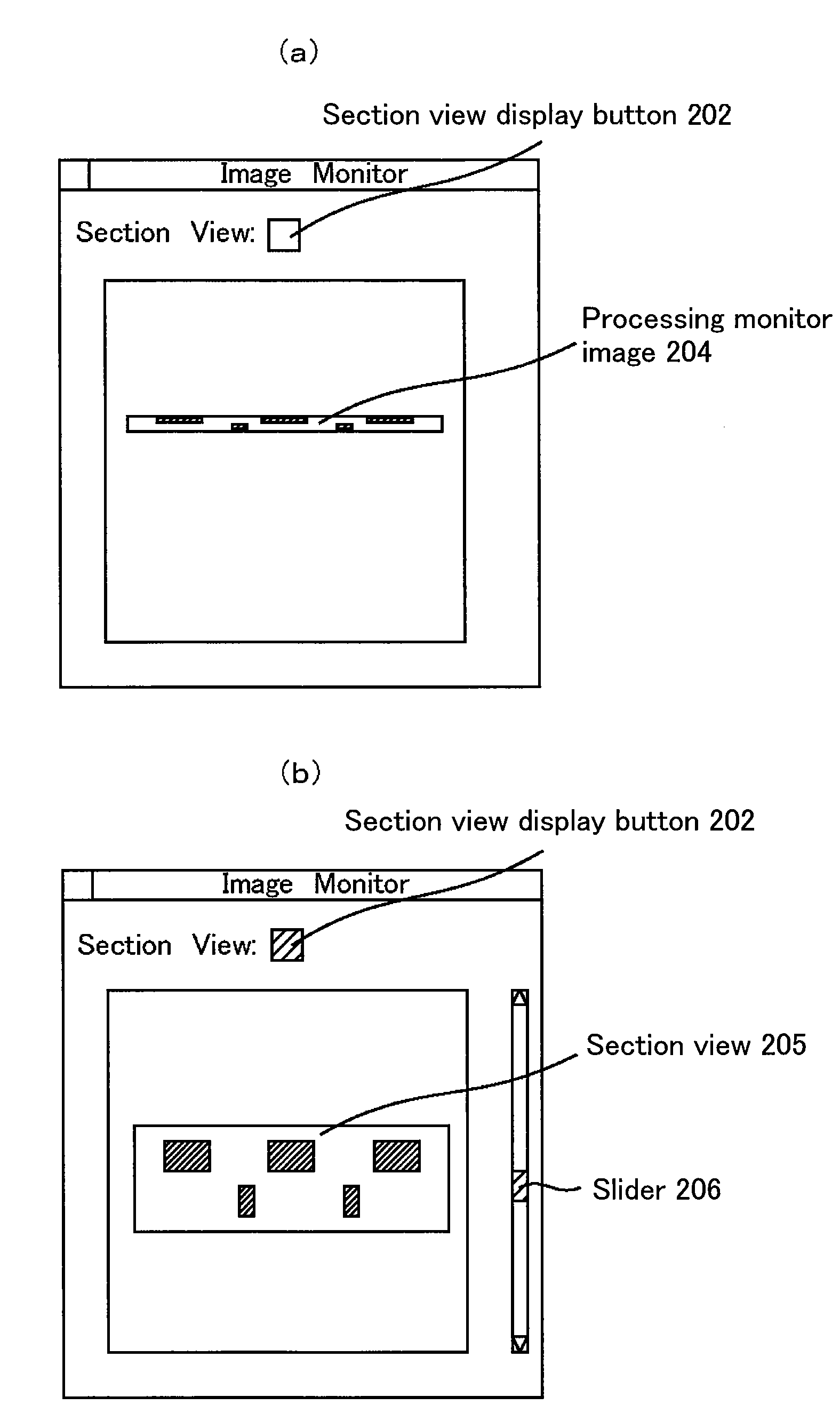
[0037]FIG. 4 shows an image monitor window used in a second embodiment. In the second embodiment, the section view function includes a function for expansion of images in the x-direction as well as the function for the expansion of images in the y-direction. Moreover, the respective expansion ratios can be set individually. Hence, the display settings can be finely adjusted to match the sample, and judgments about the processing cross-section are simplified.
[0038]FIG. 4A shows the operation state of the standard processing monitor when the zoom ratios are “1” for both the x-direction and the y-direction. FIG. 4B shows the same section view display as in the first embodiment but with a y-axis zoom ratio of “8”.
third embodiment
[0039]The third embodiment describes an example in which the manufacture and observation of a thin-film sample are performed. The apparatus which was used is a compound apparatus having an FIB column 100 and an SEM column 150 installed in a same sample chamber. A gas source 170 for performing beam induced deposition and a manipulator 140 for handling the micro-samples are also installed in the sample chamber. Moreover, a large-sample stage 160 for holding and moving a sample 1 is installed in the sample chamber. Besides the sample 1, a thin-film carrier 10 for mounting the micro-sample obtained by the sampling is also mounted on the sample stage.
[0040]FIG. 8 illustrates the (micro-sampling) method, implemented in the third embodiment, for extracting from a region to be observed. First, a first deposition film 1 is formed by FIB-induced deposition at the region of interest in the sample 1 which is fixed to the large-sample stage 160. This was performed by supplying tungsten hexacarbo...
PUM
| Property | Measurement | Unit |
|---|---|---|
| acceleration voltage | aaaaa | aaaaa |
| thickness | aaaaa | aaaaa |
| voltage | aaaaa | aaaaa |
Abstract
Description
Claims
Application Information