Hybrid fluorescent/phosphorescent oleds

a light-emitting diode and hybrid technology, applied in the direction of discharge tube/lamp details, discharge tube luminescnet screens, lamp details, etc., can solve the problems of large loss of efficiency, excitons created, and performance limitations that have been a barrier to many desirable applications, and achieve the effect of improving efficiency

Inactive Publication Date: 2008-11-20
GLOBAL OLED TECH
View PDF99 Cites 111 Cited by
  • Summary
  • Abstract
  • Description
  • Claims
  • Application Information

AI Technical Summary

Benefits of technology

[0029]The devices of the inv...

Problems solved by technology

While organic electroluminescent (EL) devices have been known for over two decades, their performance limitations have represented a barrier to many desirable applications.
However, only 25% of the excitons created in an EL device are singlet excitons.
This results in a large loss in efficiency since 75% of the excitons are not used in the light emission process.
Unfortunately, OLEDs utilizing blue phosphorescent emitters have been deficient in operational stability and therefore not suitable for most practical uses.
The potential efficiencies of these devices are limited because the triplet states formed by recombination within the fluorescent emissive layer would not be harvested as useful light.
Furthermore, it would be difficult to attain desirable CIE coordinates and CRI values for white OLED devices together with high efficiencies because the longer wavelengths from the highly efficient phosphorescent emitters would dominate the blue emission from the fluorescent emitter.
However...

Method used


Image

  • Hybrid fluorescent/phosphorescent oleds
  • Hybrid fluorescent/phosphorescent oleds
  • Hybrid fluorescent/phosphorescent oleds

Examples


examples 1-1 to 1-4

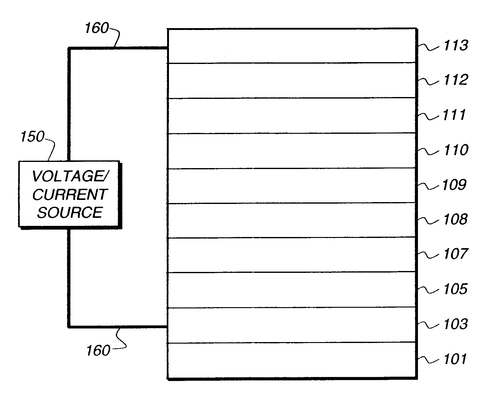
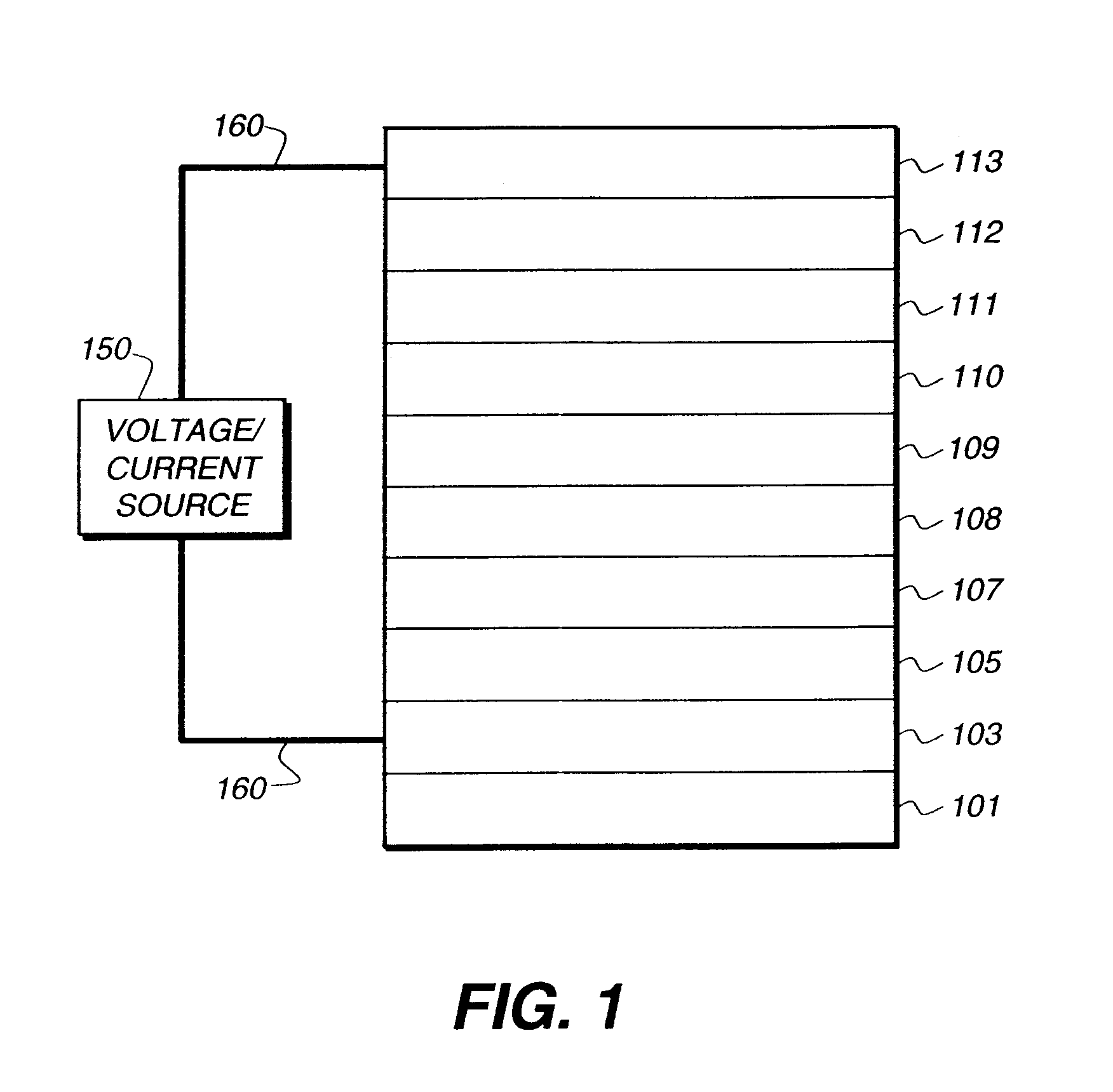
[0381]An EL device (Device 1-1) satisfying the requirements of the invention was constructed in the following manner:[0382]1. A glass substrate, coated with an approximately 25 nm layer of indium-tin oxide (ITO) as the anode, was sequentially ultrasonicated in a commercial detergent, rinsed in deionized water and exposed to an oxygen plasma for about 1 minute.[0383]2. Next, a hole transporting layer (HTL) of N,N′-di-1-naphthyl-N,N′-diphenyl-4,4′-diaminobiphenyl (Host-7 or NPB) was vacuum deposited to a thickness of 75 nm.[0384]3. An exciton / electron blocking layer (EBL) of 4,4′,4″-tris(carbazolyl)-triphenylamine (Host-6 or TCTA) was vacuum deposited to a thickness of 10 nm.[0385]4. A 5 nm light emitting layer (LEL1) consisting of a mixture of Host-8 as the host, and Emitter-1 as a blue fluorescent emitter present at concentration of 1 wt. % relative to the host was then vacuum deposited onto the exciton blocking layer.[0386]5. A spacer layer of undoped Host-2 having a thickness of 5...

examples 2-1 to 2-5

[0394]An EL device (Device 2-1) satisfying the requirements of the invention was constructed in the same manner as devices 1-1 to 1-4 with the following components: ITO / NPB (75 nm) / TCTA (10 nm) / Host-8+1% Emitter-1 (5 nm) / Host-13 (10 nm) / Host-13+8% Ir(ppy)3 (20 nm) / Bphen (25 nm) / LiF:Al

[0395]This device showed the emission from both the blue fluorescent dopant and the green phosphorescent Ir(ppy)3 dopant. At 1 mA / cm2, the luminance yield was 39.2 cd / A with CIE (x,y) of (0.232, 0.425) for an external quantum efficiency of 14.2%. The luminous yield and EQE were still higher at lower current densities. It should be noted that Host-13 (the spacer material and the phosphorescent host) has a triplet energy of 2.57 eV compared to Host-8 (2.67).

[0396]EL devices not satisfying the requirements of the invention were constructed in same manner as 2-1 except the blue fluorescent emitter was Emitter-2. The concentration was 1% in 2-2, 2% in 2-3, 5% in 2-4, and 7.5% in 2-5. Comparative example 2-2 ...

example 3-1

[0397]An EL device (Device 3-1) satisfying the requirements of the invention was constructed in the same manner as devices 1-1 to 1-4 with the following components: ITO / NPB (75 nm) / TCTA (10 nm) / Host-22+1% Emitter-1 (5 nm) / Host-13 (10 nm) / Host-13+8% Ir(ppy)3 (20 nm) / Bphen (20 nm) / LiF:Al

[0398]This device showed the emission from both the blue fluorescent dopant and the green (Ir(ppy)3) phosphorescent dopant. At 1 mA / cm2, the luminance yield was 33.2 cd / A with CIE (x,y) of (0.220, 0.380) for an external quantum efficiency of 13%. The luminous yield and EQE were still higher at lower current densities. The fluorescent host in this device has a HOMO of −5.59 eV and a triplet energy of 2.76 relative to the fluorescent emitter with a HOMO of −5.69 and the spacer material and phosphorescent host with a triplet energy of 2.57.


PUM


Abstract

An electroluminescent device comprises
    • a) a fluorescent light emitting layer comprising a fluorescent emitter and a fluorescent host material wherein the HOMO energy level of the fluorescent host material is not more than 0.1 eV more negative than that of the fluorescent emitter;
    • b) a phosphorescent light emitting layer comprising a phosphorescent emitter and a phosphorescent host material; and
    • c) a spacer layer interposed between the fluorescent light emitting layer and the phosphorescent light emitting layer;
    • wherein the triplet energy of the fluorescent host material is not more than 0.2 eV less than the triplet energy of both the spacer layer material and of the phosphorescent host material. The materials within these layers are selected so that the HOMO and triplet energy levels satisfy certain interrelationships. The invention provides devices that emit light with high luminous efficiency.

Description

CROSS REFERENCE TO RELATED APPLICATIONS[0001]This application is being co-filed with applications entitled “HYBRID OLED WITH FLUORESCENT AND PHOSPHORESCENT LAYERS”, under Attorney Docket No. 93237AEK, and “HYBRID OLED HAVING IMPROVED EFFICIENCY”, under Attorney Docket No. 93685RLO.FIELD OF THE INVENTION[0002]This invention relates to an organic light emitting diode (OLED) electroluminescent (EL) device comprising a hybrid fluorescent / phosphorescent structure wherein the blue fluorescent emission component is produced with high efficiency while simultaneously allowing energetically more favored diffusion of triplet excitons from the blue singlet emissive region to the phosphorescent emissive regions that can provide desirable electroluminescent properties such as high luminous and power efficiencies.BACKGROUND OF THE INVENTION[0003]While organic electroluminescent (EL) devices have been known for over two decades, their performance limitations have represented a barrier to many desir...

Claims


Application Information

Patent Timeline
IPC IPC(8): H01J1/62
CPCH10K85/321H10K85/324H10K85/342H10K50/131H10K50/11H10K2101/10H10K2101/27H10K85/658H10K85/322
Inventor DEATON, JOSEPH C.KONDAKOV, DENIS Y.KONDAKAVA, MARINA E.KLUBEK, KEVIN P.COMFORT, DUSTIN L.
Owner GLOBAL OLED TECH
Why Eureka
Try Eureka