Integrated transformer and method of fabrication thereof

Inactive Publication Date: 2008-11-20
CHARTERED SEMICONDUCTOR MANUFACTURING +1
View PDF15 Cites 71 Cited by
  • Summary
  • Abstract
  • Description
  • Claims
  • Application Information

AI Technical Summary

Benefits of technology

[0010]It is an aim of embodiments of the present invention

Problems solved by technology

However, power levels obtainable based on existing fully integrated amplifiers using silicon as the substrate are too low to be considered for wireless applications.
This is due to power losses caused by eddy currents induced in the silicon substrate by electromagnetic fields associated with coils of the transformer.
This technique is costly, however, and not readily compatible with foundry processing technologies.
Furthermore, additional costs are associated wit

Method used


Image

  • Integrated transformer and method of fabrication thereof
  • Integrated transformer and method of fabrication thereof
  • Integrated transformer and method of fabrication thereof

Examples


first embodiment

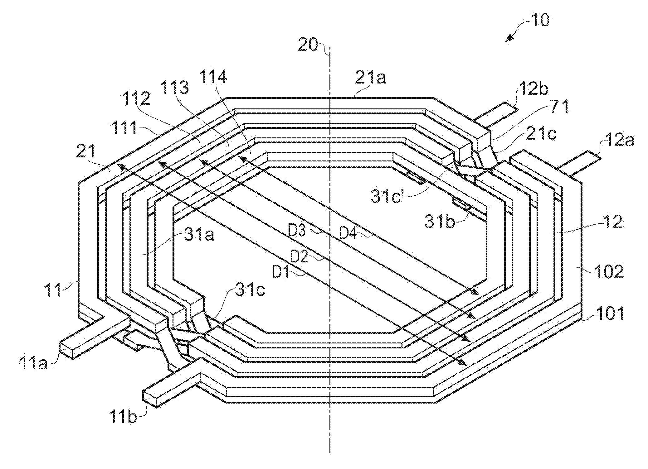
[0077]FIG. 4 shows an integrated transformer structure 10 according to the invention. The structure 10 has a primary coil 11 and a secondary coil 12. In one embodiment, each of the coils is provided with four turns through substantially 360°. Two turns of each coil are provided on each of two different lateral levels.

[0078]The primary coil 11 has a pair of terminals 11a, 11b at opposed ends of the coil. The secondary coil has a corresponding pair of terminals 12a, 12b at opposed ends. The terminals of the coils allow electrical connection of the structure to a circuit.

[0079]It will be appreciated by persons skilled in the art that embodiments of the invention are not limited to a primary coil and a secondary coil each having four turns. One or each of the coils can have a greater or smaller number of turns. Furthermore, the coils do not necessarily have to have the same number of turns.

[0080]In addition, the shape of each coil need not be the same, although advantageously the coils ...

second embodiment

[0120]FIG. 8 shows a structure 210 according to the invention.

[0121]FIG. 9 is an exploded view of the structure of FIG. 8 and shows two coils (a primary coil 211 and a secondary coil 212) that comprise the structure of FIG. 8. The primary coil has a pair of terminals 211a, 211b. The secondary coil has a corresponding pair of terminals 212a, 212b. The terminals of the coils allow electrical connection of the structure to a circuit. The primary and secondary coils each have four turns through substantially 3600.

[0122]As discussed in the context of the first embodiment, it will be appreciated by persons skilled in the art that embodiments of the invention are not limited to a primary coil and a secondary coil each having four turns. One or each of the coils of the second embodiment can have a greater or smaller number of turns. Furthermore, the coils do not necessarily have to have the same number of turns.

[0123]Furthermore, the shape of each coil need not be the same, although advanta...

third embodiment

[0166]FIG. 17 is a cross-sectional schematic diagram showing the metallisation layers used to construct an integrated transformer structure according to the invention.

[0167]In a structure according to the third embodiment, portions of a coil on the second lateral level are formed by metallisation layer TM, whilst portions of a coil on the first lateral level are formed by metallisation layer TM-1. In structures according to the first and second embodiments, portions of a coil on the second lateral level are formed by metallisation layer TM, whilst portions of a coil on the first lateral level are formed by metallisation layer TM-4. Thus, structures according to the third embodiment have the advantage that the distance between the first and second lateral levels is lower, thereby increasing the amount of electromagnetic coupling between the primary and secondary coils.

[0168]The feature of a lateral offset between contact points according to the third embodiment is illustrated in FIGS...


PUM

PropertyMeasurementUnit
Timeaaaaaaaaaa
Angleaaaaaaaaaa
Massaaaaaaaaaa

Abstract

An integrated transformer structure includes a first coil element associated with a transverse axis, the first coil element having at least one turn. The first coil element includes a first portion provided on a first lateral level, and a second portion provided on a second lateral level. The first and second lateral levels being mutually spaced apart along said transverse axis. The first and second portions being displaced laterally from said axis by different respective distances. At least one crossover portion of the first coil element, in which the first coil element being configured to provide a conducting path through at least a portion of the first portion of the first coil element to the crossover portion, through the crossover portion and subsequently through at least a portion of the second portion of the first coil element, in which any change of flow direction along said path is less than 90° in a lateral direction.

Description

FIELD OF THE INVENTION[0001]The present invention relates to integrated transformers for semiconductor integrated circuit structures, and to a method of fabricating an integrated transformer.BACKGROUND OF THE INVENTION[0002]Monolithic transformers are used in on-chip radio frequency (RF) integrated circuits (ICs) to perform a range of functions including impedance matching, signal coupling and phase splitting. Monolithic transformers provide a number of advantages for the circuit designer over conventional transformers including lower power consumption and higher packaging density. Monolithic transformers enable power amplifiers to be fabricated by standard CMOS processes. However, power levels obtainable based on existing fully integrated amplifiers using silicon as the substrate are too low to be considered for wireless applications. This is due to power losses caused by eddy currents induced in the silicon substrate by electromagnetic fields associated with coils of the transform...

Claims


Application Information

Patent Timeline
IPC IPC(8): H01F5/00
CPCH01F17/0006H01F17/0013H01F19/08Y10T29/4902H01F41/041H01L23/5227H01L2924/3011H01F27/2804H01L2924/0002H01L2924/00
Inventor LIM, CHEE CHONGCHEW, KOK WAIYEO, KIAT SENGLIM, SUH FEIDO, MANH ANHCHAN, LAP
Owner CHARTERED SEMICONDUCTOR MANUFACTURING
Why Eureka
Try Eureka