Silicon single crystal wafer and the production method

a single crystal wafer and production method technology, applied in the direction of polycrystalline material growth, silicone compounds, under protective fluid, etc., can solve the problems of minute defects called “grown-in defects” arising, affecting the quality, and outward diffusion of oxygen, etc., to achieve rapid heating and high oxide film breakdown voltage

Inactive Publication Date: 2008-11-27
SUMCO CORP
View PDF11 Cites 26 Cited by
  • Summary
  • Abstract
  • Description
  • Claims
  • Application Information

AI Technical Summary

Benefits of technology

[0016]An object of the present invention is to provide a silicon single crystal wafer capable of bringing out a gettering effect efficiently also in a thin film device and the production method.
[0019]According to the present invention, by performing a thermal treatment with rapid heating up and down for 10 seconds or shorter, COP and oxygen precipitation nuclei are eliminated though only in the surface layer area and a high oxide film breakdown voltage is exhibited in this area. Also, since high oxygen density wafer having an initial interstitial oxygen density of 1.4×10¹⁸ atoms / cc or higher is used, oxygen stable precipitation nuclei exist in an area of 10 μm or so from the surface in the wafer. Accordingly, it is possible to obtain a silicon single crystal wafer wherein crystal defects are eliminated in the wafer surface layer and stable oxygen precipitation nuclei to be gettering sources exist immediately beneath the device active region.
[0021]According to the present invention, even a wafer cut out from a crystal grown under a defect-free condition that no Grown-in defect exists when growing the crystal, since a thermal treatment with rapid heating up and down at 1000° C. or higher for 10 seconds or shorter is performed on the wafer, COP and oxygen precipitation nuclei are eliminated though only in the surface layer area and a high oxide film breakdown voltage is exhibited on this area. Also, since a wafer having a high interstitial oxygen density is used, oxygen stable precipitation nuclei exist in an area of 10 μm or so from the surface in the wafer. Accordingly, it is possible to obtain a silicon wafer wherein crystal defects are eliminated in the wafer surface layer and stable oxygen precipitation nuclei to be gettering sources exist immediately beneath the device active region.

Problems solved by technology

However, in this method, outward diffusion of oxygen is caused at the same time.
The processes include various physical treatments, chemical treatments and, furthermore, thermal treatments; and also include treatments under a severe condition of exceeding 1000° C. Therefore, a minute defect called “Grown-in defect” arises: a cause thereof is formed when growing the single crystal, becomes apparent during the production process of the device and largely affects the quality.
In this method, however, outward diffusion of oxygen is caused at the same time.
Therefore, in a wafer obtained by this method, an area without any defects called oxygen precipitate (BMD: Bulk Micro Defect) having a gettering action existing therein is formed to be as much as 10 μm or deeper from the wafer surface, and it cannot be said that a sufficient gettering capability is obtained.
The BMD having a gettering action is formed in the areas where vacancies are enriched, however, when performing a thermal treatment at 800° C. for four hours and 1000° C. for 16 hours, the BMD is formed in a deeper area than 10 μm from the wafer surface layer and formation thereof in the wafer surface layer cannot be expected.

Method used


Image

  • Silicon single crystal wafer and the production method
  • Silicon single crystal wafer and the production method
  • Silicon single crystal wafer and the production method

Examples


first embodiment

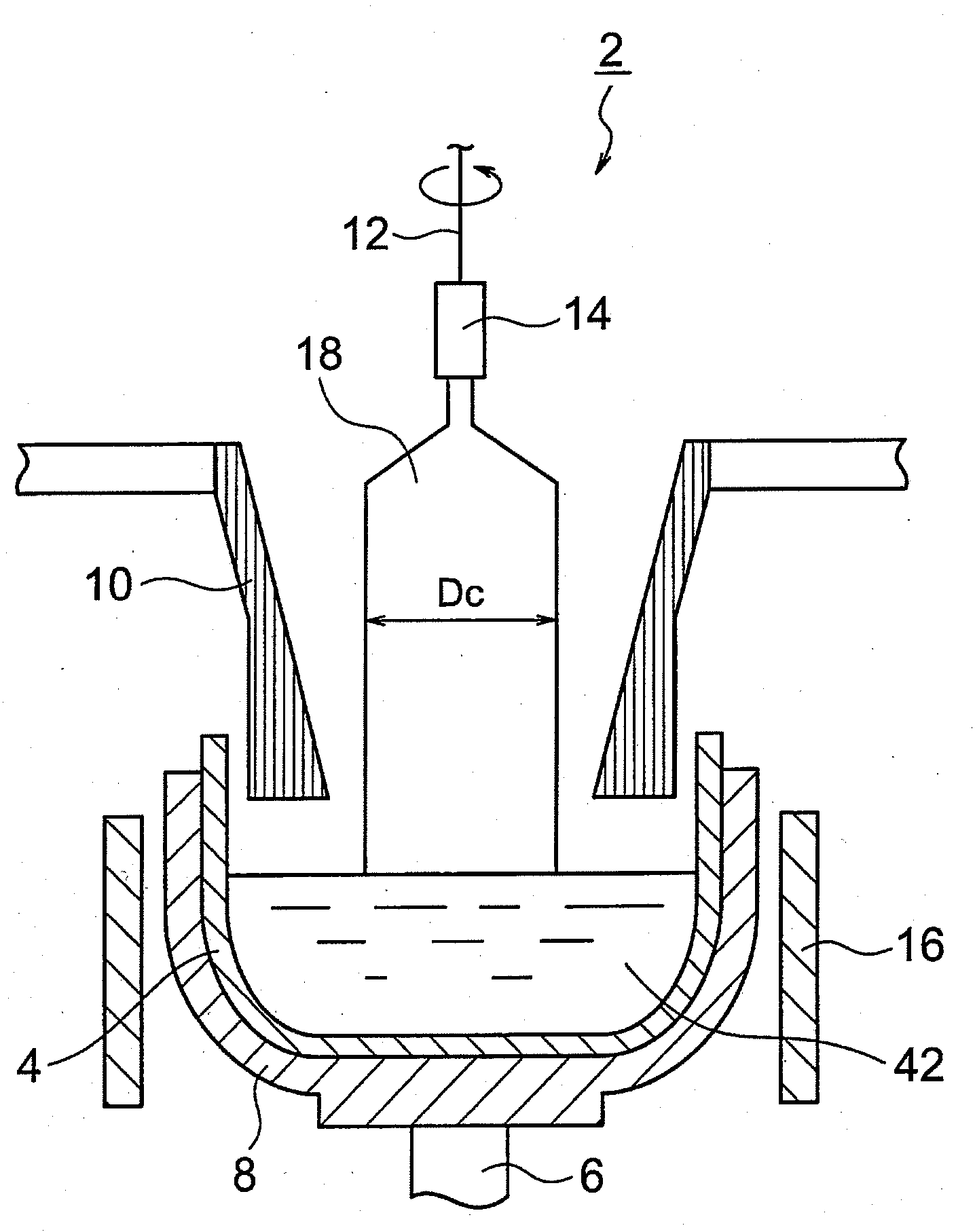
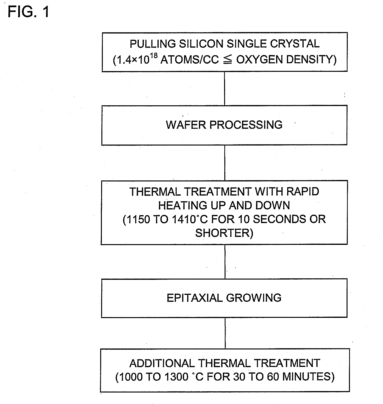
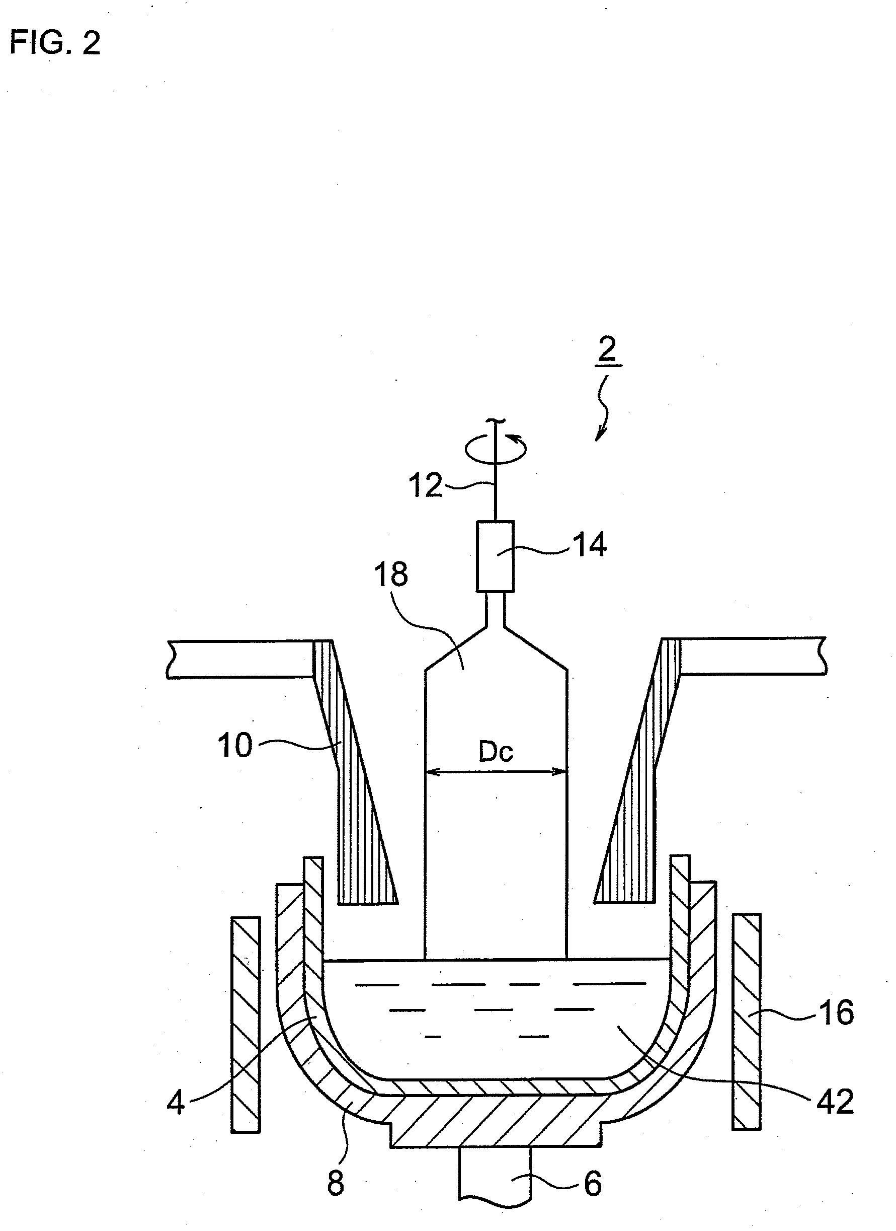
[0026]FIG. 1 is a view of a procedure of a production method of a silicon single crystal wafer according to an embodiment of the present invention. In the production method of a silicon single crystal wafer according to the present embodiment, a silicon ingot is grown by the CZ method under a condition that initial interstitial oxygen density is high as 1.4×10¹⁸ atoms / cc (ASTM F-121,1979) or higher. It is because stable oxygen precipitate to become a gettering source does not present by an effective number immediately beneath the thin film device active layer when the oxygen density at growing the silicon is lower than 1.4×10¹⁸ atoms / cc.

[0027]During the silicon growing, it is preferable to dope nitrogen in the silicon single crystal by 1×10¹³ to 1×10¹⁵ atoms / cc because the defect-free area becomes larger thereby.

[0028]Next, the silicon ingot is processed to be wafers. The wafer processing is not particularly limited and general processing methods may be used.

[0029]After the wafer pr...

example 2

[0039]Comparing with the example 1, other than changing the initial interstitial oxygen density of the silicon single crystal ingot to 22.1×10¹⁷ atoms / cc (ASTM F-121, 1979) and a condition of the thermal treatment with rapid heating up and down using a halogen lamp to 1200° C. for 3 seconds; a wafer was produced under the same condition as that in the example 1 and a defect-free depth and BMD density were measured. The results were 1.8 μm in the defect-free depth and 4.9×10⁵ pieces / cm2 in the BMD density.

example 3

[0040]Comparing with the example 1, other than changing the initial interstitial oxygen density of the silicon single crystal ingot to 14.6×10¹⁷ atoms / cc (ASTM F-121, 1979), using a flash lamp thermal treatment furnace using a xenon lamp instead of a halogen lamp and changing a condition of the thermal treatment with rapid heating up and down to 1250° C. for 0.001 second; a wafer was produced under the same condition as that in the example 1 and a defect-free depths and BMD density were measured. The results were 0.6 μm in the defect-free depth and 38.0×10⁵ pieces / cm2 in the BMD density.


PUM

PropertyMeasurementUnit
temperatureaaaaaaaaaa

Abstract

A production method of a silicon single crystal wafer capable of effectively bringing out a gettering effect also in a thin film device is provided: wherein a thermal treatment with rapid heating up and down is performed for 10 seconds or shorter on a silicon single crystal wafer obtained by processing a single crystal grown by the Czochralski method and having an initial interstitial oxygen density is 1.4×10¹⁸ atoms / cc (ASTM F-121, 1979).

Description

BACKGROUND OF THE INVENTION[0001]1. Field of the Invention[0002]The present invention relates to a silicon single crystal wafer and the production method, and particularly relates to a silicon single crystal wafer which is also suitable to a thin film device and the production method.[0003]2. Description of the Related Art[0004]In methods of producing a silicon single crystal wafer having an excellent gettering capability, there has been a proposal for eliminating COP (Crystal Originated Particles) near a surface layer of an annealed wafer by performing a thermal treatment at a temperature of 1100° C. or higher in a nonoxidizing atmosphere (refer to the Patent Article 1).[0005]However, in this method, outward diffusion of oxygen is caused at the same time. Therefore, in a wafer obtained by this method, an area with no oxygen precipitate (BMD: Bulk Micro Defect) existing therein is formed to be in a depth of 10 μm or deeper from the wafer surface.[0006]In recent years, semiconductor ...

Claims


Application Information

Patent Timeline
Patent Type & Authority Applications(United States)
IPC IPC(8): C01B33/02C30B15/00
CPCC30B15/206C30B29/06C30B15/00H01L21/208
Inventor ONO, TOSHIAKIKIHARA, TAKAYUKI
Owner SUMCO CORP
Why Eureka
Try Eureka