

Boron nitride and boron nitride-derived materials deposition method
a technology of boron nitride and materials, applied in the direction of chemical vapor deposition coating, coating, plasma technique, etc., can solve the problems of device geometries, damage to transistors, and increase the power consumed by gates
- Summary
- Abstract
- Description
- Claims
- Application Information
AI Technical Summary
Benefits of technology
Problems solved by technology
Method used
Image

Examples
Embodiment Construction
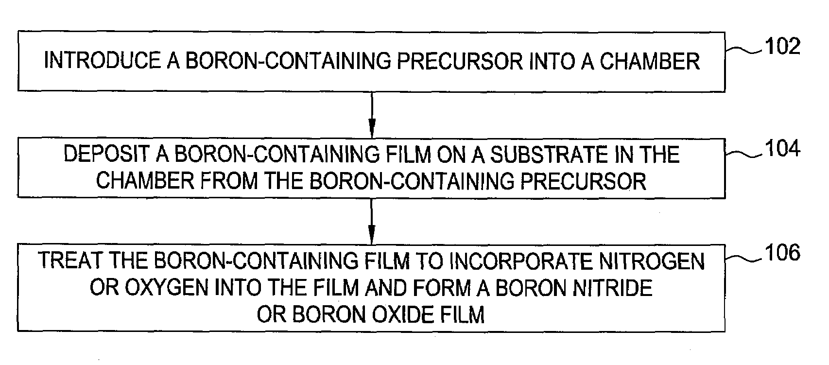
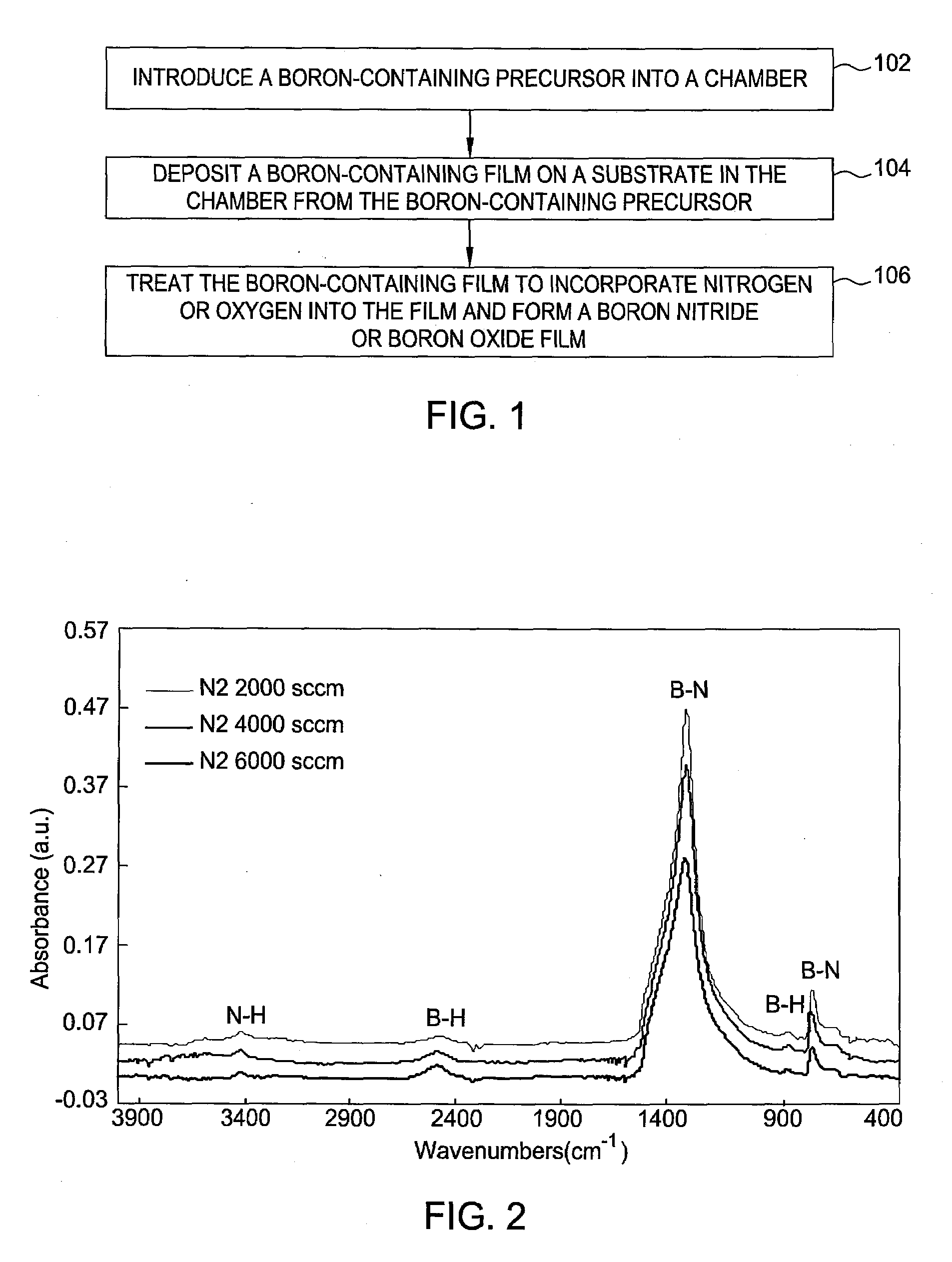
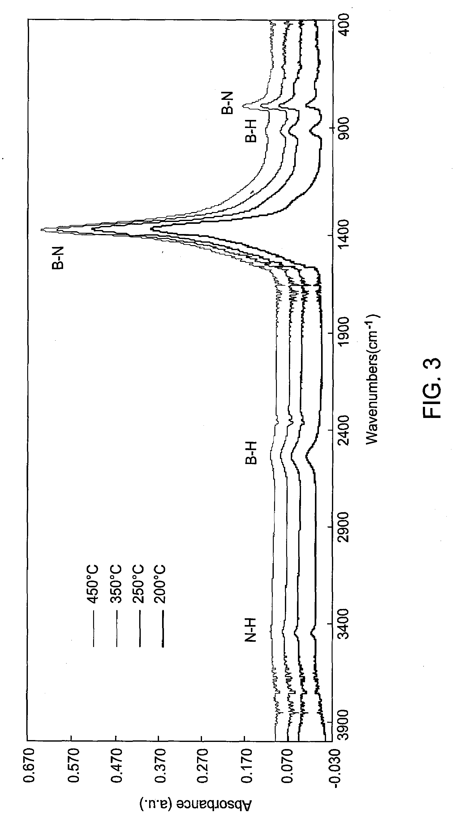
[0016]Embodiments of the present invention provide methods of depositing boron nitride, boron oxide and boron carbide films. The boron nitride, oxide and carbide films may be undoped boron nitride (BN), undoped boron oxide (B2O3) and undoped boron carbide (BC) films, or doped boron nitride, boron oxide or boron carbide films, such as boron silicon nitride (BSiN), boron silicon oxide (BSixOy), boron carbon nitride (BCN), phosphorus boron nitride (PBN), silicon boron nitride (SiBN) and boron carbon silicon nitride (BCSiN) films.
[0017]The boron nitride, boron carbide and boron oxide films may be used for front end applications, such as spacer layers and strain-inducing layers, i.e., a stress nitride layer, which is deposited to control the stress of an underlying film. The boron nitride films may have a dielectric constant between 1.1 and 10. For example, boron nitride films having a dielectric constant between 1.1 and 6.0 may be deposited by a deposition method comprising introducing ...
PUM
| Property | Measurement | Unit |
|---|---|---|
| Pressure | aaaaa | aaaaa |
| Thickness | aaaaa | aaaaa |
| Concentration | aaaaa | aaaaa |
Abstract
Description
Claims
Application Information